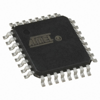
AT90LS2333-4AI Atmel, AT90LS2333-4AI Datasheet - Page 46

AT90LS2333-4AI
Manufacturer Part Number
AT90LS2333-4AI
Description
IC MCU 2K 4MHZ A/D LV IT 32TQFP
Manufacturer
Atmel
Series
AVR® 90LSr
Datasheet
1.AT90LS2333-4AC.pdf
(103 pages)
Specifications of AT90LS2333-4AI
Core Processor
AVR
Core Size
8-Bit
Speed
4MHz
Connectivity
SPI, UART/USART
Peripherals
Brown-out Detect/Reset, POR, PWM, WDT
Number Of I /o
20
Program Memory Size
2KB (1K x 16)
Program Memory Type
FLASH
Eeprom Size
128 x 8
Ram Size
128 x 8
Voltage - Supply (vcc/vdd)
2.7 V ~ 6 V
Data Converters
A/D 6x10b
Oscillator Type
Internal
Operating Temperature
-40°C ~ 85°C
Package / Case
32-TQFP, 32-VQFP
Lead Free Status / RoHS Status
Contains lead / RoHS non-compliant
The receiver front-end logic samples the signal on the RXD pin at a frequency 16 times the baud rate. While the line is idle,
one single sample of logical zero will be interpreted as the falling edge of a start bit, and the start bit detection sequence is
initiated. Let sample 1 denote the first zero-sample. Following the 1 to 0-transition, the receiver samples the RXD pin at
samples 8, 9 and 10. If two or more of these three samples are found to be logical ones, the start bit is rejected as a noise
spike and the receiver starts looking for the next 1 to 0-transition.
If however, a valid start bit is detected, sampling of the data bits following the start bit is performed. These bits are also
sampled at samples 8, 9 and 10. The logical value found in at least two of the three samples is taken as the bit value. All
bits are shifted into the transmitter shift register as they are sampled. Sampling of an incoming character is shown in Figure
42.
Figure 42. Sampling Received Data
When the stop bit enters the receiver, the majority of the three samples must be one to accept the stop bit. If two or more
samples are logical zeros, the Framing Error (FE) flag in the UART Status Register (USR) is set. Before reading the UDR
register, the user should always check the FE bit to detect Framing Errors.
Whether or not a valid stop bit is detected at the end of a character reception cycle, the data is transferred to UDR and the
RXC flag in USR is set. UDR is in fact two physically separate registers, one for transmitted data and one for received data.
When UDR is read, the Receive Data register is accessed, and when UDR is written, the Transmit Data register is
accessed. If 9 bit data word is selected (the CHR9 bit in the UART Control Register, UCR is set), the RXB8 bit in UCR is
loaded with bit 9 in the Transmit shift register when data is transferred to UDR.
If, after having received a character, the UDR register has not been read since the last receive, the OverRun (OR) flag in
UCR is set. This means that the last data byte shifted into to the shift register could not be transferred to UDR and has been
lost. The OR bit is buffered, and is updated when the valid data byte in UDR is read. Thus, the user should always check
the OR bit after reading the UDR register in order to detect any overruns if the baud rate is high or CPU load is high.
When the RXEN bit in the UCR register is cleared (zero), the receiver is disabled. This means that the PD0 pin can be used
as a general I/O pin. When RXEN is set, the UART Receiver will be connected to PD0, which is forced to be an input pin
regardless of the setting of the DDD0 bit in DDRD. When PD0 is forced to input by the UART, the PORTD0 bit can still be
used to control the pull-up resistor on the pin.
When the CHR9 bit in the UCR register is set, transmitted and received characters are 9-bit long plus start and stop bits.
The 9th data bit to be transmitted is the TXB8 bit in UCR register. This bit must be set to the wanted value before a trans-
mission is initated by writing to the UDR register. The 9th data bit received is the RXB8 bit in the UCR register.
Multi-Processor Communication Mode
The Multi-Processor Communication Mode enables several slave MCUs to receive data from a master MCU. This is done
by first decoding an address byte to find out which MCU has been addressed. If a particular slave MCU has been
addressed, it will receive the following data bytes as normal, while the other slave MCUs will ignore the data bytes until
another address byte is received.
For an MCU to act as a master MCU, it should enter 9-bit transmission mode (CHR9 in UCSRB set). The 9th bit must be
one to indicate that an address byte is being transmitted, and zero to indicate that a data byte is being transmitted.
For the slave MCUs, the mechanism appears slightly differently for 8-bit and 9-bit reception mode. In 8-bit reception mode
(CHR9 in UCSRB cleared), the stop bit is one for an address byte and zero for a data byte. In 9-bit reception mode (CHR9
in UCSRB set), the 9th bit is one for an address byte and zero for a data byte, whereas the stop bit is always high.
The following procedure should be used to exchange data in Multi-Processor Communication Mode:
1. All slave MCUs are in Multi-Processor Communication Mode (MPCM in UCSRA is set).
2. The master MCU sends an address byte, and all slaves receive and read this byte. In the slave MCUs, the RXC flag
in UCSRA will be set as normal.
AT90S/LS2333 and AT90S/LS4433
46


