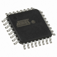
AT90LS2333-4AI Atmel, AT90LS2333-4AI Datasheet - Page 55

AT90LS2333-4AI
Manufacturer Part Number
AT90LS2333-4AI
Description
IC MCU 2K 4MHZ A/D LV IT 32TQFP
Manufacturer
Atmel
Series
AVR® 90LSr
Datasheet
1.AT90LS2333-4AC.pdf
(103 pages)
Specifications of AT90LS2333-4AI
Core Processor
AVR
Core Size
8-Bit
Speed
4MHz
Connectivity
SPI, UART/USART
Peripherals
Brown-out Detect/Reset, POR, PWM, WDT
Number Of I /o
20
Program Memory Size
2KB (1K x 16)
Program Memory Type
FLASH
Eeprom Size
128 x 8
Ram Size
128 x 8
Voltage - Supply (vcc/vdd)
2.7 V ~ 6 V
Data Converters
A/D 6x10b
Oscillator Type
Internal
Operating Temperature
-40°C ~ 85°C
Package / Case
32-TQFP, 32-VQFP
Lead Free Status / RoHS Status
Contains lead / RoHS non-compliant
Figure 48. ADC Timing Diagram, Free Run Conversion
ADC Noise Canceler Function
The ADC features a noise canceler that enables conversion during idle mode to reduce noise induced from the CPU core.
To make use of this feature, the following procedure should be used:
1. Make sure that the ADC is enabled and is not busy converting. Single Conversion Mode must be selected and the
2. Enter idle mode. The ADC will start a conversion once the CPU has been halted.
3. If no other interrupts occur before the ADC conversion completes, the ADC interrupt will wake up the MCU and exe-
ADC Multiplexer Select Register - ADMUX
•
These bits are reserved bits in the AT90S2333/4433, and should be written to zero if accessed.
•
When this bit is set and the BOD is enabled (BODEN fuse is programmed), a fixed bandgap voltage of 1.22 ± 0.05V
replaces the normal input to the ADC. When this bit is cleared, the normal input pin (as selected by MUX2..MUX0) is
applied to the ADC.
•
These bits are reserved bits in the AT90S2333/4433, and should be written to zero if accessed.
•
The value of these three bits selects which analog input 5-0 is connected to the ADC.
Bit
$07 ($27)
Read/Write
Initial value
Bit 7 - Res: Reserved Bits
Bit 6 - ADCBG: ADC Bandgap Select
Bit 5..3 - Res: Reserved Bits
Bits 2..0 - MUX2..MUX0: Analog Channel Select Bits 2-0
ADC conversion complete interrupt must be enabled. Thus:
ADEN = 1
ADSC = 0
ADFR = 0
ADIE = 1
cute the ADC conversion complete interrupt routine.
R
7
0
-
ADCBG
R/W
6
0
Cycle number
ADC clock
ADSC
Hold strobe
ADIF
ADCH
ADCL
R
5
0
-
R
4
0
-
One Conversion
11
AT90S/LS2333 and AT90S/LS4433
R
3
0
-
12
13
MUX2
R/W
2
0
Next
Conversion
1
MSB of result
LSB of result
MUX1
2
R/W
1
0
MUX0
R/W
0
0
ADMUX
55


