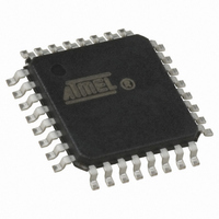
AT90LS2333-4AI Atmel, AT90LS2333-4AI Datasheet - Page 34

AT90LS2333-4AI
Manufacturer Part Number
AT90LS2333-4AI
Description
IC MCU 2K 4MHZ A/D LV IT 32TQFP
Manufacturer
Atmel
Series
AVR® 90LSr
Datasheet
1.AT90LS2333-4AC.pdf
(103 pages)
Specifications of AT90LS2333-4AI
Core Processor
AVR
Core Size
8-Bit
Speed
4MHz
Connectivity
SPI, UART/USART
Peripherals
Brown-out Detect/Reset, POR, PWM, WDT
Number Of I /o
20
Program Memory Size
2KB (1K x 16)
Program Memory Type
FLASH
Eeprom Size
128 x 8
Ram Size
128 x 8
Voltage - Supply (vcc/vdd)
2.7 V ~ 6 V
Data Converters
A/D 6x10b
Oscillator Type
Internal
Operating Temperature
-40°C ~ 85°C
Package / Case
32-TQFP, 32-VQFP
Lead Free Status / RoHS Status
Contains lead / RoHS non-compliant
Timer/Counter1 Output Compare Register - OCR1H and OCR1L
The output compare register is a 16-bit read/write register.
The Timer/Counter1 Output Compare Register contains the data to be continuously compared with Timer/Counter1.
Actions on compare matches are specified in the Timer/Counter1 Control and Status register.
Since the Output Compare Register - OCR1 - is a 16-bit register, a temporary register TEMP is used when OCR1 is written
to ensure that both bytes are updated simultaneously. When the CPU writes the high byte, OCR1H, the data is temporarily
stored in the TEMP register. When the CPU writes the low byte, OCR1L, the TEMP register is simultaneously written to
OCR1H. Consequently, the high byte OCR1H must be written first for a full 16-bit register write operation.
The TEMP register is also used when accessing TCNT1, and ICR1. If the main program and also interrupt routines perform
access to registers using TEMP, interrupts must be disabled during access from the main program.
Timer/Counter1 Input Capture Register - ICR1H and ICR1L
The input capture register is a 16-bit read-only register.
When the rising or falling edge (according to the input capture edge setting - ICES1) of the signal at the input capture pin -
ICP - is detected, the current value of the Timer/Counter1 is transferred to the Input Capture Register - ICR1. At the same
time, the input capture flag - ICF1 - is set (one).
Since the Input Capture Register - ICR1 - is a 16-bit register, a temporary register TEMP is used when ICR1 is read to
ensure that both bytes are read simultaneously. When the CPU reads the low byte ICR1L, the data is sent to the CPU and
the data of the high byte ICR1H is placed in the TEMP register. When the CPU reads the data in the high byte ICR1H, the
CPU receives the data in the TEMP register. Consequently, the low byte ICR1L must be accessed first for a full 16-bit reg-
ister read operation.
The TEMP register is also used when accessing TCNT1 and OCR1. If the main program and also interrupt routines per-
form access to registers using TEMP, interrupts must be disabled during access from the main program.
Timer/Counter1 in PWM mode
When the PWM mode is selected, Timer/Counter1 and the Output Compare Register1 - OCR1, form a 8, 9, or 10-bit, free-
running, glitch-free, and phase correct PWM with output on the PB1(OC1) pin. Timer/Counter1 acts as an up/down
counter, counting up from $0000 to TOP (see Table 13), where it turns and counts down again to zero before the cycle is
repeated. When the counter value matches the contents of the 8, 9 or 10 least significant bits of OCR1, the PB1(OC1) pin
34
Bit
$2B ($4B)
$2A ($4A)
Read/Write
Initial value
Bit
$27 ($47)
$26 ($46)
Read/Write
Initial value
AT90S/LS2333 and AT90S/LS4433
MSB
MSB
R/W
R/W
15
15
R
R
7
0
0
7
0
0
R/W
R/W
14
14
R
R
6
0
0
6
0
0
R/W
R/W
13
13
R
R
5
0
0
5
0
0
R/W
R/W
12
12
R
R
4
0
0
4
0
0
R/W
R/W
11
11
R
R
3
0
0
3
0
0
R/W
R/W
10
10
R
R
2
0
0
2
0
0
R/W
R/W
R
R
9
1
0
0
9
1
0
0
LSB
R/W
R/W
LSB
R
R
8
0
0
0
8
0
0
0
OCR1H
OCR1L
ICR1H
ICR1L


