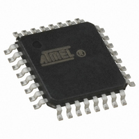
AT90LS2333-4AI Atmel, AT90LS2333-4AI Datasheet - Page 4

AT90LS2333-4AI
Manufacturer Part Number
AT90LS2333-4AI
Description
IC MCU 2K 4MHZ A/D LV IT 32TQFP
Manufacturer
Atmel
Series
AVR® 90LSr
Datasheet
1.AT90LS2333-4AC.pdf
(103 pages)
Specifications of AT90LS2333-4AI
Core Processor
AVR
Core Size
8-Bit
Speed
4MHz
Connectivity
SPI, UART/USART
Peripherals
Brown-out Detect/Reset, POR, PWM, WDT
Number Of I /o
20
Program Memory Size
2KB (1K x 16)
Program Memory Type
FLASH
Eeprom Size
128 x 8
Ram Size
128 x 8
Voltage - Supply (vcc/vdd)
2.7 V ~ 6 V
Data Converters
A/D 6x10b
Oscillator Type
Internal
Operating Temperature
-40°C ~ 85°C
Package / Case
32-TQFP, 32-VQFP
Lead Free Status / RoHS Status
Contains lead / RoHS non-compliant
Pin Descriptions
VCC
Supply voltage
GND
Ground
Port B (PB5..PB0)
Port B is a 6-bit bi-directional I/O port with internal pullup resistors. The Port B output buffers can sink 20 mA. As inputs,
Port B pins that are externally pulled low will source current if the pull-up resistors are activated.
Port B also serves the functions of various special features of the AT90S2333/4433 as listed on page 60.
The port B pins are tristated when a reset condition becomes active, even if the clock is not running.
Port C (PC5..PC0)
Port C is a 6-bit bi-directional I/O port with internal pullup resistors. The Port C output buffers can sink 20 mA. As inputs,
Port C pins that are externally pulled low will source current if the pull-up resistors are activated. Port C also serves as the
analog inputs to the A/D Converter.
The port C pins are tristated when a reset condition becomes active, even if the clock is not running.
Port D (PD7..PD0)
Port D is an 8-bit bi-directional I/O port with internal pull-up resistors. The Port D output buffers can sink 20 mA. As inputs,
Port D pins that are externally pulled low will source current if the pull-up resistors are activated.
Port D also serves the functions of various special features of the AT90S2333/4433 as listed on page 67.
The port D pins are tristated when a reset condition becomes active, even if the clock is not running.
RESET
Reset input. An external reset is generated by a low level on the RESET pin. Reset pulses longer than 50 ns will generate
a reset, even if the clock is not running. Shorter pulses are not guaranteed to generate a reset.
XTAL1
Input to the inverting oscillator amplifier and input to the internal clock operating circuit.
XTAL2
Output from the inverting oscillator amplifier
AVCC
This is the supply voltage pin for the A/D Converter. It should be externally connected to V
via a low-pass filter. See
CC
page 52 for details on operation of the ADC.
AREF
This is the analog reference input for the A/D Converter. For ADC operations, a voltage in the range 2.7V to AVCC must be
applied to this pin.
AGND
If the board has a separate analog ground plane, this pin should be connected to this ground plane. Otherwise, connect to
GND.
AT90S/LS2333 and AT90S/LS4433
4


