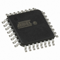
AT90LS2333-4AI Atmel, AT90LS2333-4AI Datasheet - Page 26

AT90LS2333-4AI
Manufacturer Part Number
AT90LS2333-4AI
Description
IC MCU 2K 4MHZ A/D LV IT 32TQFP
Manufacturer
Atmel
Series
AVR® 90LSr
Datasheet
1.AT90LS2333-4AC.pdf
(103 pages)
Specifications of AT90LS2333-4AI
Core Processor
AVR
Core Size
8-Bit
Speed
4MHz
Connectivity
SPI, UART/USART
Peripherals
Brown-out Detect/Reset, POR, PWM, WDT
Number Of I /o
20
Program Memory Size
2KB (1K x 16)
Program Memory Type
FLASH
Eeprom Size
128 x 8
Ram Size
128 x 8
Voltage - Supply (vcc/vdd)
2.7 V ~ 6 V
Data Converters
A/D 6x10b
Oscillator Type
Internal
Operating Temperature
-40°C ~ 85°C
Package / Case
32-TQFP, 32-VQFP
Lead Free Status / RoHS Status
Contains lead / RoHS non-compliant
MCU Control Register - MCUCR
The MCU Control Register contains control bits for general MCU functions.
•
These bits are reserved bits in the AT90S2333/4433 and always reads as zero.
•
The SE bit must be set (one) to make the MCU enter the sleep mode when the SLEEP instruction is executed. To avoid the
MCU entering the sleep mode unless it is the programmers purpose, it is recommended to set the Sleep Enable SE bit just
before the execution of the SLEEP instruction.
•
This bit selects between the two available sleep modes. When SM is cleared (zero), Idle Mode is selected as sleep mode.
When SM is set (one), Power Down Mode is selected as Sleep Mode. For details, refer to the paragraph “Sleep Modes”
below.
•
The External Interrupt 1 is activated by the external pin INT1 if the SREG I-flag and the corresponding interrupt mask in the
GIMSK is set. The level and edges on the external INT1 pin that activate the interrupt are defined in the following table:
Table 7. Interrupt 1 Sense Control
Note:
The value on the INT1 pin is sampled before detecting edges. If edge or toggle interrupt is selected, pulses that last longer
than one clock period will generate an interrupt. Shorter pulses are not guaranteed to generate an interrupt. If low level
interrupt is selected, the low level must be held until the completion of the currently executing instruction to generate an
interrupt
•
The External Interrupt 0 is activated by the external pin INT0 if the SREG I-flag and the corresponding interrupt mask is set.
The level and edges on the external INT0 pin that activate the interrupt are defined in the following table:
Table 8. Interrupt 0 Sense Control
Note:
26
Bit
$35 ($55)
Read/Write
Initial value
Bits 7, 6 - Res: Reserved bit
Bit 5 - SE: Sleep Enable
Bits 4 - SM: Sleep Mode
Bits 3, 2 - ISC11, ISC10: Interrupt Sense Control 1 bit 1 and bit 0
Bits 1, 0 - ISC01, ISC00: Interrupt Sense Control 0 bit 1 and bit 0
ISC01
ISC11
When changing the ISC11/ISC10 bits, INT1 must be disabled by clearing its Interrupt Enable bit in the GIMSK Register. Other-
wise an interrupt can occur when the bits are changed.
When changing the ISC01/ISC00 bits, INT0 must be disabled by clearing its Interrupt Enable bit in the GIMSK Register. Other-
wise an interrupt can occur when the bits are changed.
0
0
1
1
0
0
1
1
AT90S/LS2333 and AT90S/LS4433
R
7
0
-
ISC00
0
1
0
1
R
6
0
-
ISC10
0
1
0
1
R/W
SE
5
0
Description
The low level of INT0 generates an interrupt request.
Any logical change on INT0 generates an interrupt request.
The falling edge of INT0 generates an interrupt request.
The rising edge of INT0 generates an interrupt request.
Description
The low level of INT1 generates an interrupt request.
Any logical change on INT1 generates an interrupt request.
The falling edge of INT1 generates an interrupt request.
The rising edge of INT1 generates an interrupt request.
R/W
SM
4
0
ISC11
R/W
3
0
ISC10
R/W
2
0
ISC01
R/W
1
0
ISC00
R/W
0
0
MCUCR


