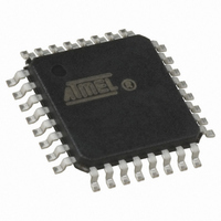
AT90LS2333-4AI Atmel, AT90LS2333-4AI Datasheet - Page 73

AT90LS2333-4AI
Manufacturer Part Number
AT90LS2333-4AI
Description
IC MCU 2K 4MHZ A/D LV IT 32TQFP
Manufacturer
Atmel
Series
AVR® 90LSr
Datasheet
1.AT90LS2333-4AC.pdf
(103 pages)
Specifications of AT90LS2333-4AI
Core Processor
AVR
Core Size
8-Bit
Speed
4MHz
Connectivity
SPI, UART/USART
Peripherals
Brown-out Detect/Reset, POR, PWM, WDT
Number Of I /o
20
Program Memory Size
2KB (1K x 16)
Program Memory Type
FLASH
Eeprom Size
128 x 8
Ram Size
128 x 8
Voltage - Supply (vcc/vdd)
2.7 V ~ 6 V
Data Converters
A/D 6x10b
Oscillator Type
Internal
Operating Temperature
-40°C ~ 85°C
Package / Case
32-TQFP, 32-VQFP
Lead Free Status / RoHS Status
Contains lead / RoHS non-compliant
Table 30. Pin Name Mapping
Table 31. XA1 and XA0 Coding
Table 32. Command Byte Bit Coding
Enter Programming Mode
The following algorithm puts the device in parallel programming mode:
1. Apply supply voltage according to Table 29, between V
2. Set the RESET and BS pin to ‘0’ and wait at least 100 ns.
3. Apply 11.5 - 12.5V to RESET. Any activity on BS within 100 ns after +12V has been applied to RESET, will cause
Chip Erase
The Chip Erase command will erase the Flash and EEPROM memories, and the Lock bits. The Lock bits are not reset until
the Flash and EEPROM have been completely erased. The Fuse bits are not changed. Chip Erase must be performed
before the Flash or EEPROM is reprogrammed.
Load Command “Chip Erase”
Signal Name in Programming Mode
XA1
the device to fail entering programming mode.
0
0
1
1
XA0
0
1
0
1
RDY/BSY
DATA
XA0
XA1
WR
OE
BS
Command Byte
1000 0000
0100 0000
0010 0000
0001 0000
0001 0001
0000 1000
0000 0100
0000 0010
0000 0011
Action when XTAL1 is Pulsed
Load Flash or EEPROM Address (High or low address byte determined by BS)
Load Data (High or Low data byte for Flash determined by BS)
Load Command
No Action, Idle
PC1-0, PB5-0
Pin Name
PD1
PD2
PD3
PD4
PD5
PD6
Command Executed
Chip Erase
Write Fuse Bits
Write Lock Bits
Write Flash
Write EEPROM
Read Signature Bytes
Read Fuse and Lock Bits
Read Flash
Read EEPROM
I/O
I/O
O
AT90S/LS2333 and AT90S/LS4433
I
I
I
I
I
CC
Function
0: Device is busy programming, 1: Device is ready for new command
Output Enable (Active low)
Write Pulse (Active low)
Byte Select (‘0’ selects low byte, ‘1’ selects high byte)
XTAL Action Bit 0
XTAL Action Bit 1
Bidirectional Databus (Output when OE is low)
and GND.
73


