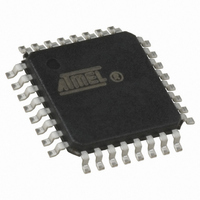
AT90LS2333-4AI Atmel, AT90LS2333-4AI Datasheet - Page 67

AT90LS2333-4AI
Manufacturer Part Number
AT90LS2333-4AI
Description
IC MCU 2K 4MHZ A/D LV IT 32TQFP
Manufacturer
Atmel
Series
AVR® 90LSr
Datasheet
1.AT90LS2333-4AC.pdf
(103 pages)
Specifications of AT90LS2333-4AI
Core Processor
AVR
Core Size
8-Bit
Speed
4MHz
Connectivity
SPI, UART/USART
Peripherals
Brown-out Detect/Reset, POR, PWM, WDT
Number Of I /o
20
Program Memory Size
2KB (1K x 16)
Program Memory Type
FLASH
Eeprom Size
128 x 8
Ram Size
128 x 8
Voltage - Supply (vcc/vdd)
2.7 V ~ 6 V
Data Converters
A/D 6x10b
Oscillator Type
Internal
Operating Temperature
-40°C ~ 85°C
Package / Case
32-TQFP, 32-VQFP
Lead Free Status / RoHS Status
Contains lead / RoHS non-compliant
Table 27. DDDn Bits on Port D Pins
Note:
Alternate Functions Of Port D
•
AIN1, Analog Comparator Negative Input. When configured as an input (DDD7 is cleared (zero)) and with the internal MOS
pull up resistor switched off (PD7 is cleared (zero)), this pin also serves as the negative input of the on-chip analog compar-
ator. During power down mode, the schmitt trigger of the digital input is disconnected. This allows analog signals which are
close to V
•
AIN0, Analog Comparator Positive Input. When configured as an input (DDD6 is cleared (zero)) and with the internal MOS
pull up resistor switched off (PD6 is cleared (zero)), this pin also serves as the positive input of the on-chip analog compar-
ator. During power down mode, the schmitt trigger of the digital input is disconnected. This allows analog signals which are
close to V
•
T1, Timer/Counter1 counter source. See the timer description for further details
•
T0: Timer/Counter0 counter source. See the timer description for further details.
•
INT1, External Interrupt source 1: The PD3 pin can serve as an external interrupt source to the MCU. See the interrupt
description for further details, and how to enable the source.
•
INT0, External Interrupt source 0: The PD2 pin can serve as an external interrupt source to the MCU. See the interrupt
description for further details, and how to enable the source.
•
Transmit Data (Data output pin for the UART). When the UART transmitter is enabled, this pin is configured as an output
regardless of the value of DDD1.
•
Receive Data (Data input pin for the UART). When the UART receiver is enabled this pin is configured as an input regard-
less of the value of DDD0. When the UART forces this pin to be an input, a logical one in PORTD0 will turn on the internal
pull-up.
AIN1 - Port D, Bit 7
AIN0 - Port D, Bit 6
T1 - Port D, Bit 5
T0 - Port D, Bit 4
INT1 - Port D, Bit 3
INT0 - Port D, Bit 2
TXD - Port D, Bit 1
RXD - Port D, Bit 0
DDDn
0
0
1
1
n: 7,6…0, pin number.
CC
CC
/2 to be present during power down without causing excessive power consumption.
/2 to be present during power down without causing excessive power consumption.
PORTDn
0
1
0
1
Output
Output
Input
Input
I/O
Pull Up
Yes
No
No
No
AT90S/LS2333 and AT90S/LS4433
Comment
Tri-state (Hi-Z)
PDn will source current if ext. pulled low.
Push-Pull Zero Output
Push-Pull One Output
67


