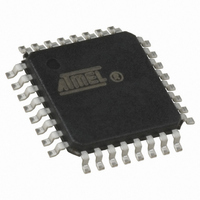
AT90LS2333-4AI Atmel, AT90LS2333-4AI Datasheet - Page 74

AT90LS2333-4AI
Manufacturer Part Number
AT90LS2333-4AI
Description
IC MCU 2K 4MHZ A/D LV IT 32TQFP
Manufacturer
Atmel
Series
AVR® 90LSr
Datasheet
1.AT90LS2333-4AC.pdf
(103 pages)
Specifications of AT90LS2333-4AI
Core Processor
AVR
Core Size
8-Bit
Speed
4MHz
Connectivity
SPI, UART/USART
Peripherals
Brown-out Detect/Reset, POR, PWM, WDT
Number Of I /o
20
Program Memory Size
2KB (1K x 16)
Program Memory Type
FLASH
Eeprom Size
128 x 8
Ram Size
128 x 8
Voltage - Supply (vcc/vdd)
2.7 V ~ 6 V
Data Converters
A/D 6x10b
Oscillator Type
Internal
Operating Temperature
-40°C ~ 85°C
Package / Case
32-TQFP, 32-VQFP
Lead Free Status / RoHS Status
Contains lead / RoHS non-compliant
1. Set XA1, XA0 to ‘10’. This enables command loading.
2. Set BS to ‘0’.
3. Set DATA to ‘1000 0000’. This is the command for Chip erase.
4. Give XTAL1 a positive pulse. This loads the command.
5. Give WR a
wide negative pulse to execute Chip Erase. See Table 33 for
value. Chip Erase does not
t
t
WLWH_CE
WLWH_CE
generate any activity on the RDY/BSY pin.
Programming the Flash
A: Load Command “Write Flash”
1. Set XA1, XA0 to ‘10’. This enables command loading.
2. Set BS to ‘0’
3. Set DATA to ‘0001 0000’. This is the command for Write Flash.
4. Give XTAL1 a positive pulse. This loads the command.
B: Load Address High Byte
1. Set XA1, XA0 to ‘00’. This enables address loading.
2. Set BS to ‘1’. This selects high byte.
3. Set DATA = Address high byte ($00 - $03/$07)
4. Give XTAL1 a positive pulse. This loads the address high byte.
C: Load Address Low Byte
1. Set XA1, XA0 to ‘00’. This enables address loading.
2. Set BS to ‘0’. This selects low byte.
3. Set DATA = Address low byte ($00 - $FF)
4. Give XTAL1 a positive pulse. This loads the address low byte.
D: Load Data Low Byte
1. Set XA1, XA0 to ‘01’. This enables data loading.
2. Set DATA = Data low byte ($00 - $FF)
3. Give XTAL1 a positive pulse. This loads the data low byte.
E: Write Data Low Byte
1. Set BS to ‘0’. This selects low data.
2. Give WR a negative pulse. This starts programming of the data byte. RDY/BSY goes low.
3. Wait until RDY/BSY goes high to program the next byte.
(See Figure 63 for signal waveforms.)
F: Load Data High Byte
1. Set XA1, XA0 to ‘01’. This enables data loading.
2. Set DATA = Data high byte ($00 - $FF)
3. Give XTAL1 a positive pulse. This loads the data high byte.
G: Write Data High Byte
1. Set BS to ‘1’. This selects high data.
2. Give WR a negative pulse. This starts programming of the data byte. RDY/BSY goes low.
3. Wait until RDY/BSY goes high to program the next byte.
(See Figure 64 for signal waveforms.)
The loaded command and address are retained in the device during programming. For efficient programming, the following
should be considered.
• The command needs only be loaded once when writing or reading multiple memory locations.
AT90S/LS2333 and AT90S/LS4433
74


