ATTINY167-15XD Atmel, ATTINY167-15XD Datasheet - Page 120
ATTINY167-15XD
Manufacturer Part Number
ATTINY167-15XD
Description
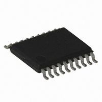
MCU AVR 16K FLASH 15MHZ 20-TSSOP
Manufacturer
Atmel
Series
AVR® ATtinyr
Datasheet
1.ATTINY167-15MD.pdf
(283 pages)
Specifications of ATTINY167-15XD
Core Processor
AVR
Core Size
8-Bit
Speed
16MHz
Connectivity
I²C, LIN, SPI, UART/USART, USI
Peripherals
Brown-out Detect/Reset, POR, PWM, Temp Sensor, WDT
Number Of I /o
16
Program Memory Size
16KB (8K x 16)
Program Memory Type
FLASH
Eeprom Size
512 x 8
Ram Size
512 x 8
Voltage - Supply (vcc/vdd)
2.7 V ~ 5.5 V
Data Converters
A/D 11x10b
Oscillator Type
Internal
Operating Temperature
-40°C ~ 150°C
Package / Case
20-TSSOP
Processor Series
ATTINY1x
Core
AVR8
Data Bus Width
8 bit
Data Ram Size
512 B
Maximum Clock Frequency
16 MHz
Maximum Operating Temperature
+ 85 C
Mounting Style
SMD/SMT
3rd Party Development Tools
EWAVR, EWAVR-BL
Development Tools By Supplier
ATAVRDRAGON, ATSTK500, ATSTK600, ATAVRISP2, ATAVRONEKIT
Minimum Operating Temperature
- 40 C
For Use With
ATSTK600-SOIC - STK600 SOCKET/ADAPTER FOR SOIC
Lead Free Status / RoHS Status
Lead free / RoHS Compliant


12.7.1
12.7.2
12.7.3
12.8
120
Compare Match Output Unit
ATtiny87/ATtiny167
Force Output Compare
Compare Match Blocking by TCNT1 Write
Using the Output Compare Unit
The OCR1A/B Register access may seem complex, but this is not case. When the double
buffering is enabled, the CPU has access to the OCR1A/B Buffer Register, and if double buff-
ering is disabled the CPU will access the OCR1A/B directly. The content of the OCR1A/B
(Buffer or Compare) Register is only changed by a write operation (the Timer/Counter does
not update this register automatically as the TCNT1 and ICR1 Register). Therefore OCR1A/B
is not read via the high byte temporary register (TEMP). However, it is a good practice to read
the low byte first as when accessing other 16-bit registers. Writing the OCR1A/B Registers
must be done via the TEMP Register since the compare of all 16 bits is done continuously.
The high byte (OCR1A/BH) has to be written first. When the high byte I/O location is written by
the CPU, the TEMP Register will be updated by the value written. Then when the low byte
(OCR1A/BL) is written to the lower eight bits, the high byte will be copied into the upper 8-bits
of either the OCR1A/B buffer or OCR1A/B Compare Register in the same system clock cycle.
For more information of how to access the 16-bit registers refer to
on page
In non-PWM Waveform Generation modes, the match output of the comparator can be forced
by writing a one to the Force Output Compare (FOC1A/B) bit. Forcing compare match will not
set the OCF1A/B flag or reload/clear the timer, but the OC1A/Bi pins will be updated as if a
real compare match had occurred (the COM1A/B1:0 bits settings define whether the OC1A/Bi
pins are set, cleared or toggled - if the respective OCnxi bit is set).
All CPU writes to the TCNT1 Register will block any compare match that occurs in the next
timer clock cycle, even when the timer is stopped. This feature allows OCR1A/B to be initial-
ized to the same value as TCNT1 without triggering an interrupt when the Timer/Counter clock
is enabled.
Since writing TCNT1 in any mode of operation will block all compare matches for one timer
clock cycle, there are risks involved when changing TCNT1 when using any of the Output
Compare channels, independent of whether the Timer/Counter is running or not. If the value
written to TCNT1 equals the OCR1A/B value, the compare match will be missed, resulting in
incorrect waveform generation. Do not write the TCNT1 equal to TOP in PWM modes with
variable TOP values. The compare match for the TOP will be ignored and the counter will con-
tinue to 0xFFFF. Similarly, do not write the TCNT1 value equal to BOTTOM when the counter
is downcounting.
The setup of the OC1A/B should be performed before setting the Data Direction Register for
the port pin to output. The easiest way of setting the OC1A/B value is to use the Force Output
Compare (FOC1A/B) strobe bits in Normal mode. The OC1A/B Register keeps its value even
when changing between Waveform Generation modes.
Be aware that the COM1A/B1:0 bits are not double buffered together with the compare value.
Changing the COM1A/B1:0 bits will take effect immediately.
The Compare Output mode (COM1A/B1:0) bits have two functions. The Waveform Generator
uses the COM1A/B1:0 bits for defining the Output Compare (OC1A/B) state at the next com-
pare match. Secondly the COM1A/B1:0 and OCnxi bits control the OC1A/Bi pin output source.
112.
“Accessing 16-bit Registers”
7728G–AVR–06/10
Related parts for ATTINY167-15XD
Image
Part Number
Description
Manufacturer
Datasheet
Request
R

Part Number:
Description:
Manufacturer:
Atmel Corporation
Datasheet:
Part Number:
Description:
Manufacturer:
Atmel Corporation
Datasheet:

Part Number:
Description:
MCU AVR 16K FLASH 15MHZ 32-QFN
Manufacturer:
Atmel
Datasheet:

Part Number:
Description:
IC MCU AVR 16K FLASH 20TSSOP
Manufacturer:
Atmel
Datasheet:
Part Number:
Description:
MCU AVR 16K FLASH 15MHZ 32-QFN
Manufacturer:
Atmel
Datasheet:

Part Number:
Description:
MCU AVR 16K FLASH 15MHZ 20-SOIC
Manufacturer:
Atmel
Datasheet:

Part Number:
Description:
MCU AVR 16K FLASH 15MHZ 20-TSSOP
Manufacturer:
Atmel
Datasheet:
Part Number:
Description:
IC MCU AVR 16K FLASH 20SOIC
Manufacturer:
Atmel
Datasheet: