ATTINY167-15XD Atmel, ATTINY167-15XD Datasheet - Page 94
ATTINY167-15XD
Manufacturer Part Number
ATTINY167-15XD
Description
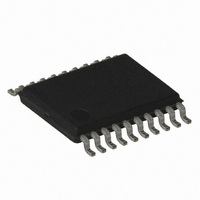
MCU AVR 16K FLASH 15MHZ 20-TSSOP
Manufacturer
Atmel
Series
AVR® ATtinyr
Datasheet
1.ATTINY167-15MD.pdf
(283 pages)
Specifications of ATTINY167-15XD
Core Processor
AVR
Core Size
8-Bit
Speed
16MHz
Connectivity
I²C, LIN, SPI, UART/USART, USI
Peripherals
Brown-out Detect/Reset, POR, PWM, Temp Sensor, WDT
Number Of I /o
16
Program Memory Size
16KB (8K x 16)
Program Memory Type
FLASH
Eeprom Size
512 x 8
Ram Size
512 x 8
Voltage - Supply (vcc/vdd)
2.7 V ~ 5.5 V
Data Converters
A/D 11x10b
Oscillator Type
Internal
Operating Temperature
-40°C ~ 150°C
Package / Case
20-TSSOP
Processor Series
ATTINY1x
Core
AVR8
Data Bus Width
8 bit
Data Ram Size
512 B
Maximum Clock Frequency
16 MHz
Maximum Operating Temperature
+ 85 C
Mounting Style
SMD/SMT
3rd Party Development Tools
EWAVR, EWAVR-BL
Development Tools By Supplier
ATAVRDRAGON, ATSTK500, ATSTK600, ATAVRISP2, ATAVRONEKIT
Minimum Operating Temperature
- 40 C
For Use With
ATSTK600-SOIC - STK600 SOCKET/ADAPTER FOR SOIC
Lead Free Status / RoHS Status
Lead free / RoHS Compliant


10.7.3
94
ATtiny87/ATtiny167
Fast PWM Mode
For generating a waveform output in CTC mode, the OC0A output can be set to toggle its log-
ical level on each compare match by setting the Compare Output mode bits to toggle mode
(COM0A1:0 = 1). The OC0A value will not be visible on the port pin unless the data direction
for the pin is set to output. The waveform generated will have a maximum frequency of f
f
ing equation:
The N variable represents the prescale factor (1, 8, 32, 64, 128, 256, or 1024).
As for the Normal mode of operation, the TOV0 flag is set in the same timer clock cycle that
the counter counts from MAX to 0x00.
The fast Pulse Width Modulation or fast PWM mode (WGM01:0 = 3) provides a high frequency
PWM waveform generation option. The fast PWM differs from the other PWM option by its sin-
gle-slope operation. The counter counts from BOTTOM to MAX then restarts from BOTTOM.
In non-inverting Compare Output mode, the Output Compare (OC0A) is cleared on the com-
pare match between TCNT0 and OCR0A, and set at BOTTOM. In inverting Compare Output
mode, the output is set on compare match and cleared at BOTTOM. Due to the single-slope
operation, the operating frequency of the fast PWM mode can be twice as high as the phase
correct PWM mode that uses dual-slope operation. This high frequency makes the fast PWM
mode well suited for power regulation, rectification, and DAC applications. High frequency
allows physically small sized external components (coils, capacitors), and therefore reduces
total system cost.
In fast PWM mode, the counter is incremented until the counter value matches the MAX value.
The counter is then cleared at the following timer clock cycle. The timing diagram for the fast
PWM mode is shown in
histogram for illustrating the single-slope operation. The diagram includes non-inverted and
inverted PWM outputs. The small horizontal line marks on the TCNT0 slopes represent com-
pare matches between OCR0A and TCNT0.
Figure 10-6. Fast PWM Mode, Timing Diagram
clk_I/O
TCNTn
OCnx
OCnx
Period
/2 when OCR0A is set to zero (0x00). The waveform frequency is defined by the follow-
1
2
Figure
3
10-6. The TCNT0 value is in the timing diagram shown as a
f
OCnx
4
=
------------------------------------------------------ -
2
N
5
f
clk_I/O
1
+
6
OCRnx
7
OCRnx Interrupt Flag Set
OCRnx Update and
TOVn Interrupt Flag Set
(COMnx1:0 = 2)
(COMnx1:0 = 3)
7728G–AVR–06/10
OC
0
A
=
Related parts for ATTINY167-15XD
Image
Part Number
Description
Manufacturer
Datasheet
Request
R

Part Number:
Description:
Manufacturer:
Atmel Corporation
Datasheet:
Part Number:
Description:
Manufacturer:
Atmel Corporation
Datasheet:

Part Number:
Description:
MCU AVR 16K FLASH 15MHZ 32-QFN
Manufacturer:
Atmel
Datasheet:

Part Number:
Description:
IC MCU AVR 16K FLASH 20TSSOP
Manufacturer:
Atmel
Datasheet:
Part Number:
Description:
MCU AVR 16K FLASH 15MHZ 32-QFN
Manufacturer:
Atmel
Datasheet:

Part Number:
Description:
MCU AVR 16K FLASH 15MHZ 20-SOIC
Manufacturer:
Atmel
Datasheet:

Part Number:
Description:
MCU AVR 16K FLASH 15MHZ 20-TSSOP
Manufacturer:
Atmel
Datasheet:
Part Number:
Description:
IC MCU AVR 16K FLASH 20SOIC
Manufacturer:
Atmel
Datasheet: