ATTINY167-15XD Atmel, ATTINY167-15XD Datasheet - Page 31
ATTINY167-15XD
Manufacturer Part Number
ATTINY167-15XD
Description
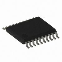
MCU AVR 16K FLASH 15MHZ 20-TSSOP
Manufacturer
Atmel
Series
AVR® ATtinyr
Datasheet
1.ATTINY167-15MD.pdf
(283 pages)
Specifications of ATTINY167-15XD
Core Processor
AVR
Core Size
8-Bit
Speed
16MHz
Connectivity
I²C, LIN, SPI, UART/USART, USI
Peripherals
Brown-out Detect/Reset, POR, PWM, Temp Sensor, WDT
Number Of I /o
16
Program Memory Size
16KB (8K x 16)
Program Memory Type
FLASH
Eeprom Size
512 x 8
Ram Size
512 x 8
Voltage - Supply (vcc/vdd)
2.7 V ~ 5.5 V
Data Converters
A/D 11x10b
Oscillator Type
Internal
Operating Temperature
-40°C ~ 150°C
Package / Case
20-TSSOP
Processor Series
ATTINY1x
Core
AVR8
Data Bus Width
8 bit
Data Ram Size
512 B
Maximum Clock Frequency
16 MHz
Maximum Operating Temperature
+ 85 C
Mounting Style
SMD/SMT
3rd Party Development Tools
EWAVR, EWAVR-BL
Development Tools By Supplier
ATAVRDRAGON, ATSTK500, ATSTK600, ATAVRISP2, ATAVRONEKIT
Minimum Operating Temperature
- 40 C
For Use With
ATSTK600-SOIC - STK600 SOCKET/ADAPTER FOR SOIC
Lead Free Status / RoHS Status
Lead free / RoHS Compliant


4.2.7
4.3
4.3.1
7728G–AVR–06/10
Dynamic Clock Switch
Clock Output Buffer
Features
Table 4-9.
Notes:
Note that the System Clock Prescaler can be used to implement run-time changes of the inter-
nal clock frequency while still ensuring stable operation. Refer to
page 37
If not using a crystal oscillator, the device can output the system clock on the CLKO pin. To
enable the output, the CKOUT Fuse or COUT bit of CLKSELR register has to be programmed.
This option is useful when the device clock is needed to drive other circuits on the system.
Note that the clock will not be output during reset and the normal operation of I/O pin will be
overridden when the fuses are programmed. If the System Clock Prescaler is used, it is the
divided system clock that is output.
The ATtiny87/167 provides a powerful dynamic clock switch circuit that allows users to turn on
and off clocks of the device on the fly. The built-in de-glitching circuitry allows clocks to be
enabled or disabled asynchronously. This enables efficient power management schemes to
be implemented easily and quickly. In a safety application, the dynamic clock switch circuit
allows continuous monitoring of the external clock permitting a fallback scheme in case of
clock failure.
The control of the dynamic clock switch circuit must be supervised by software. This operation
is facilitated by the following features:
• Safe commands, to avoid unintentional commands, a special write procedure must be
• Exclusive action, the actions are controlled by a decoding table (commands) written to the
CSUT1..0
SUT1..0
followed to change the CLKCSR register bits
page
CLKCSR register. This ensures that only one command operation can be launched at any
time. The main actions of the decoding table are:
– ‘Disable Clock Source’,
– ‘Enable Clock Source’,
– ‘Request Clock Availability’,
– ‘Clock Source Switching’,
00
01
10
11
1. Flash Fuse bits.
2. CLKSELR register bits.
3. Additional delay (+ 4ms) available if RSTDISBL fuse is set.
for details.
38.):
(1)
(2)
Start-up Times for the External Clock Selection
Start-up Time from
Power-down/save
6 CK
6 CK
6 CK
Additional Delay from Reset
14CK (+ 4.1 ms
14CK + 4.1 ms
14CK + 65 ms
(Vcc = 5.0V)
(See “CLKPR – Clock Prescaler Register” on
Reserved
ATtiny87/ATtiny167
(3)
)
“System Clock Prescaler” on
Recommended Usage
BOD enabled
Fast rising power
Slowly rising power
31
Related parts for ATTINY167-15XD
Image
Part Number
Description
Manufacturer
Datasheet
Request
R

Part Number:
Description:
Manufacturer:
Atmel Corporation
Datasheet:
Part Number:
Description:
Manufacturer:
Atmel Corporation
Datasheet:

Part Number:
Description:
MCU AVR 16K FLASH 15MHZ 32-QFN
Manufacturer:
Atmel
Datasheet:

Part Number:
Description:
IC MCU AVR 16K FLASH 20TSSOP
Manufacturer:
Atmel
Datasheet:
Part Number:
Description:
MCU AVR 16K FLASH 15MHZ 32-QFN
Manufacturer:
Atmel
Datasheet:

Part Number:
Description:
MCU AVR 16K FLASH 15MHZ 20-SOIC
Manufacturer:
Atmel
Datasheet:

Part Number:
Description:
MCU AVR 16K FLASH 15MHZ 20-TSSOP
Manufacturer:
Atmel
Datasheet:
Part Number:
Description:
IC MCU AVR 16K FLASH 20SOIC
Manufacturer:
Atmel
Datasheet: