ATTINY167-15XD Atmel, ATTINY167-15XD Datasheet - Page 38
ATTINY167-15XD
Manufacturer Part Number
ATTINY167-15XD
Description
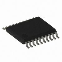
MCU AVR 16K FLASH 15MHZ 20-TSSOP
Manufacturer
Atmel
Series
AVR® ATtinyr
Datasheet
1.ATTINY167-15MD.pdf
(283 pages)
Specifications of ATTINY167-15XD
Core Processor
AVR
Core Size
8-Bit
Speed
16MHz
Connectivity
I²C, LIN, SPI, UART/USART, USI
Peripherals
Brown-out Detect/Reset, POR, PWM, Temp Sensor, WDT
Number Of I /o
16
Program Memory Size
16KB (8K x 16)
Program Memory Type
FLASH
Eeprom Size
512 x 8
Ram Size
512 x 8
Voltage - Supply (vcc/vdd)
2.7 V ~ 5.5 V
Data Converters
A/D 11x10b
Oscillator Type
Internal
Operating Temperature
-40°C ~ 150°C
Package / Case
20-TSSOP
Processor Series
ATTINY1x
Core
AVR8
Data Bus Width
8 bit
Data Ram Size
512 B
Maximum Clock Frequency
16 MHz
Maximum Operating Temperature
+ 85 C
Mounting Style
SMD/SMT
3rd Party Development Tools
EWAVR, EWAVR-BL
Development Tools By Supplier
ATAVRDRAGON, ATSTK500, ATSTK600, ATAVRISP2, ATAVRONEKIT
Minimum Operating Temperature
- 40 C
For Use With
ATSTK600-SOIC - STK600 SOCKET/ADAPTER FOR SOIC
Lead Free Status / RoHS Status
Lead free / RoHS Compliant


4.5.2
38
ATtiny87/ATtiny167
CLKPR – Clock Prescaler Register
the range. Incrementing CAL6..0 by 1 will give a frequency increment of less than 2% in the
frequency range 7.3 - 8.1 MHz.
• Bit 7 – CLKPCE: Clock Prescaler Change Enable
The CLKPCE bit must be written to logic one to enable change of the CLKPS bits. The CLK-
PCE bit is only updated when the other bits in CLKPR are simultaneously written to zero.
CLKPCE is cleared by hardware four cycles after it is written or when the CLKPS bits are writ-
ten. Rewriting the CLKPCE bit within this time-out period does neither extend the time-out
period, nor clear the CLKPCE bit.
• Bits 6:4 – Res: Reserved Bits
These bits are reserved bits in the ATtiny87/167 and will always read as zero.
• Bits 3:0 – CLKPS3:0: Clock Prescaler Select Bits 3 - 0
These bits define the division factor between the selected clock source and the internal sys-
tem clock. These bits can be written run-time to vary the clock frequency to suit the application
requirements. As the divider divides the master clock input to the MCU, the speed of all syn-
chronous peripherals is reduced when a division factor is used. The division factors are given
in
To avoid unintentional changes of clock frequency, a special write procedure must be followed
to change the CLKPS bits:
Interrupts must be disabled when changing prescaler setting in order not to disturb the
procedure.
The CKDIV8 Fuse determines the initial value of the CLKPS bits. If CKDIV8 is unprogrammed,
the CLKPS bits will be reset to “0000”. If CKDIV8 is programmed, CLKPS bits are reset to
“0011”, giving a division factor of eight at start up. This feature should be used if the selected
clock source has a higher frequency than the maximum frequency of the device at the present
operating conditions. Note that any value can be written to the CLKPS bits regardless of the
CKDIV8 Fuse setting. The Application software must ensure that a sufficient division factor is
chosen if the selected clock source has a higher frequency than the maximum frequency of
the device at the present operating conditions. The device is shipped with the CKDIV8 Fuse
programmed.
Bit
Read/Write
Initial Value
1. Write the Clock Prescaler Change Enable (CLKPCE) bit to one and all other bits in
2. Within four cycles, write the desired value to CLKPS while writing a zero to CLKPCE.
Table
CLKPR to zero.
4-10.
CLKPCE
R/W
7
0
R
6
–
0
R
5
–
0
R
4
–
0
CLKPS3
R/W
3
CLKPS2
See Bit Description
R/W
2
CLKPS1
R/W
1
CLKPS0
R/W
0
7728G–AVR–06/10
CLKPR
Related parts for ATTINY167-15XD
Image
Part Number
Description
Manufacturer
Datasheet
Request
R

Part Number:
Description:
Manufacturer:
Atmel Corporation
Datasheet:
Part Number:
Description:
Manufacturer:
Atmel Corporation
Datasheet:

Part Number:
Description:
MCU AVR 16K FLASH 15MHZ 32-QFN
Manufacturer:
Atmel
Datasheet:

Part Number:
Description:
IC MCU AVR 16K FLASH 20TSSOP
Manufacturer:
Atmel
Datasheet:
Part Number:
Description:
MCU AVR 16K FLASH 15MHZ 32-QFN
Manufacturer:
Atmel
Datasheet:

Part Number:
Description:
MCU AVR 16K FLASH 15MHZ 20-SOIC
Manufacturer:
Atmel
Datasheet:

Part Number:
Description:
MCU AVR 16K FLASH 15MHZ 20-TSSOP
Manufacturer:
Atmel
Datasheet:
Part Number:
Description:
IC MCU AVR 16K FLASH 20SOIC
Manufacturer:
Atmel
Datasheet: