ATTINY167-15XD Atmel, ATTINY167-15XD Datasheet - Page 236
ATTINY167-15XD
Manufacturer Part Number
ATTINY167-15XD
Description
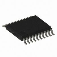
MCU AVR 16K FLASH 15MHZ 20-TSSOP
Manufacturer
Atmel
Series
AVR® ATtinyr
Datasheet
1.ATTINY167-15MD.pdf
(283 pages)
Specifications of ATTINY167-15XD
Core Processor
AVR
Core Size
8-Bit
Speed
16MHz
Connectivity
I²C, LIN, SPI, UART/USART, USI
Peripherals
Brown-out Detect/Reset, POR, PWM, Temp Sensor, WDT
Number Of I /o
16
Program Memory Size
16KB (8K x 16)
Program Memory Type
FLASH
Eeprom Size
512 x 8
Ram Size
512 x 8
Voltage - Supply (vcc/vdd)
2.7 V ~ 5.5 V
Data Converters
A/D 11x10b
Oscillator Type
Internal
Operating Temperature
-40°C ~ 150°C
Package / Case
20-TSSOP
Processor Series
ATTINY1x
Core
AVR8
Data Bus Width
8 bit
Data Ram Size
512 B
Maximum Clock Frequency
16 MHz
Maximum Operating Temperature
+ 85 C
Mounting Style
SMD/SMT
3rd Party Development Tools
EWAVR, EWAVR-BL
Development Tools By Supplier
ATAVRDRAGON, ATSTK500, ATSTK600, ATAVRISP2, ATAVRONEKIT
Minimum Operating Temperature
- 40 C
For Use With
ATSTK600-SOIC - STK600 SOCKET/ADAPTER FOR SOIC
Lead Free Status / RoHS Status
Lead free / RoHS Compliant


21.7.9
21.7.10
21.7.11
236
ATtiny87/ATtiny167
Programming the Fuse High Bits
Programming the Extended Fuse Bits
Programming the Lock Bits
PAGEL / BS1
RESET +12V
The algorithm for programming the Fuse High bits is as follows (refer to
Flash” on page 232
The algorithm for programming the Extended Fuse bits is as follows (refer to
the Flash” on page 232
Figure 21-5. Programming the FUSES Waveforms
The algorithm for programming the Lock bits is as follows (refer to
page 232
XA1 / BS2
RDY/BSY
1. A: Load Command “0100 0000
2. C: Load Data Low Byte. Bit n = “0” programs and bit n = “1” erases the Fuse bit.
3. Set BS1 to “1” and BS2 to “0”. This selects high data byte.
4. Give WR a negative pulse and wait for RDY/BSY to go high.
5. Set BS1 to “0”. This selects low data byte.
1. A: Load Command “0100 0000
2. C: Load Data Low Byte. Bit n = “0” programs and bit n = “1” erases the Fuse bit.
3. Set BS1 to “0” and BS2 to “1”. This selects extended data byte.
4. Give WR a negative pulse and wait for RDY/BSY to go high.
5. Set BS2 to “0”. This selects low data byte.
1. A: Load Command “0010 0000
2. C: Load Data Low Byte. Bit n = “0” programs the Lock bit. If LB mode 3 is pro-
3. Give WR a negative pulse and wait for RDY/BSY to go high.
4. The Lock bits can only be cleared by executing Chip Erase.
XTAL1
DATA
XA0
WR
OE
grammed (LB1 and LB2 is programmed), it is not possible to re-program the Lock bits
by any External Programming mode.
for details on Command and Data loading):
0x40
A
DATA
C
for details on Command and Data loading):
Write Fuse Low byte
for details on Command and Data loading):
XX
b
b
b
”.
”.
”.
0x40
A
DATA
C
Write Fuse high byte
XX
“Programming the Flash” on
0x40
A
Write Extended Fuse byte
DATA
“Programming the
C
“Programming
7728G–AVR–06/10
XX
Related parts for ATTINY167-15XD
Image
Part Number
Description
Manufacturer
Datasheet
Request
R

Part Number:
Description:
Manufacturer:
Atmel Corporation
Datasheet:
Part Number:
Description:
Manufacturer:
Atmel Corporation
Datasheet:

Part Number:
Description:
MCU AVR 16K FLASH 15MHZ 32-QFN
Manufacturer:
Atmel
Datasheet:

Part Number:
Description:
IC MCU AVR 16K FLASH 20TSSOP
Manufacturer:
Atmel
Datasheet:
Part Number:
Description:
MCU AVR 16K FLASH 15MHZ 32-QFN
Manufacturer:
Atmel
Datasheet:

Part Number:
Description:
MCU AVR 16K FLASH 15MHZ 20-SOIC
Manufacturer:
Atmel
Datasheet:

Part Number:
Description:
MCU AVR 16K FLASH 15MHZ 20-TSSOP
Manufacturer:
Atmel
Datasheet:
Part Number:
Description:
IC MCU AVR 16K FLASH 20SOIC
Manufacturer:
Atmel
Datasheet: