ATTINY167-15XD Atmel, ATTINY167-15XD Datasheet - Page 231
ATTINY167-15XD
Manufacturer Part Number
ATTINY167-15XD
Description
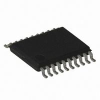
MCU AVR 16K FLASH 15MHZ 20-TSSOP
Manufacturer
Atmel
Series
AVR® ATtinyr
Datasheet
1.ATTINY167-15MD.pdf
(283 pages)
Specifications of ATTINY167-15XD
Core Processor
AVR
Core Size
8-Bit
Speed
16MHz
Connectivity
I²C, LIN, SPI, UART/USART, USI
Peripherals
Brown-out Detect/Reset, POR, PWM, Temp Sensor, WDT
Number Of I /o
16
Program Memory Size
16KB (8K x 16)
Program Memory Type
FLASH
Eeprom Size
512 x 8
Ram Size
512 x 8
Voltage - Supply (vcc/vdd)
2.7 V ~ 5.5 V
Data Converters
A/D 11x10b
Oscillator Type
Internal
Operating Temperature
-40°C ~ 150°C
Package / Case
20-TSSOP
Processor Series
ATTINY1x
Core
AVR8
Data Bus Width
8 bit
Data Ram Size
512 B
Maximum Clock Frequency
16 MHz
Maximum Operating Temperature
+ 85 C
Mounting Style
SMD/SMT
3rd Party Development Tools
EWAVR, EWAVR-BL
Development Tools By Supplier
ATAVRDRAGON, ATSTK500, ATSTK600, ATAVRISP2, ATAVRONEKIT
Minimum Operating Temperature
- 40 C
For Use With
ATSTK600-SOIC - STK600 SOCKET/ADAPTER FOR SOIC
Lead Free Status / RoHS Status
Lead free / RoHS Compliant


21.7
21.7.1
21.7.2
21.7.3
7728G–AVR–06/10
Parallel Programming
Enter Programming Mode
Considerations for Efficient Programming
Chip Erase
The following algorithm puts the device in parallel programming mode:
The loaded command and address are retained in the device during programming. For effi-
cient programming, the following should be considered.
The Chip Erase will erase the Flash and EEPROM
bits are not reset until the program memory has been completely erased. The Fuse bits are
not changed. A Chip Erase must be performed before the Flash and/or EEPROM are
reprogrammed.
Note:
Load Command “Chip Erase”
1. Apply 4.5 - 5.5V between Vcc and GND.
2. Set RESET to “0” and toggle XTAL1 at least six times.
3. Set the Prog_enable pins listed in
4. Apply 11.5 - 12.5V to RESET. Any activity on Prog_enable pins within 100 ns after
5. Wait at least 50 µs before sending a new command.
• The command needs only be loaded once when writing or reading multiple memory
• Skip writing the data value 0xFF, that is the contents of the entire EEPROM (unless the
• Address high byte needs only be loaded before programming or reading a new 256 word
1. Set XA1, XA0 to “1,0 ”. This enables command loading.
2. Set BS1 to “0”.
3. Set DATA to “1000 0000
4. Give XTAL1 a positive pulse. This loads the command.
5. Give WR a negative pulse. This starts the Chip Erase. RDY/BSY goes low.
6. Wait until RDY/BSY goes high before loading a new command.
locations.
EESAVE Fuse is programmed) and Flash after a Chip Erase.
window in Flash or 256 byte EEPROM. This consideration also applies to Signature bytes
reading.
least 100 ns.
+12V has been applied to RESET, will cause the device to fail entering programming
mode.
The EEPRPOM memory is preserved during Chip Erase if the EESAVE Fuse is programmed.
b
”. This is the command for Chip Erase.
Table 21-10 on page 230
(Note:)
ATtiny87/ATtiny167
memories plus Lock bits. The Lock
to “0000
b
” and wait at
231
Related parts for ATTINY167-15XD
Image
Part Number
Description
Manufacturer
Datasheet
Request
R

Part Number:
Description:
Manufacturer:
Atmel Corporation
Datasheet:
Part Number:
Description:
Manufacturer:
Atmel Corporation
Datasheet:

Part Number:
Description:
MCU AVR 16K FLASH 15MHZ 32-QFN
Manufacturer:
Atmel
Datasheet:

Part Number:
Description:
IC MCU AVR 16K FLASH 20TSSOP
Manufacturer:
Atmel
Datasheet:
Part Number:
Description:
MCU AVR 16K FLASH 15MHZ 32-QFN
Manufacturer:
Atmel
Datasheet:

Part Number:
Description:
MCU AVR 16K FLASH 15MHZ 20-SOIC
Manufacturer:
Atmel
Datasheet:

Part Number:
Description:
MCU AVR 16K FLASH 15MHZ 20-TSSOP
Manufacturer:
Atmel
Datasheet:
Part Number:
Description:
IC MCU AVR 16K FLASH 20SOIC
Manufacturer:
Atmel
Datasheet: