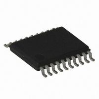
ATTINY167-15XD Atmel, ATTINY167-15XD Datasheet - Page 149

ATTINY167-15XD
Manufacturer Part Number
ATTINY167-15XD
Description
MCU AVR 16K FLASH 15MHZ 20-TSSOP
Manufacturer
Atmel
Series
AVR® ATtinyr
Datasheet
1.ATTINY167-15MD.pdf
(283 pages)
Specifications of ATTINY167-15XD
Core Processor
AVR
Core Size
8-Bit
Speed
16MHz
Connectivity
I²C, LIN, SPI, UART/USART, USI
Peripherals
Brown-out Detect/Reset, POR, PWM, Temp Sensor, WDT
Number Of I /o
16
Program Memory Size
16KB (8K x 16)
Program Memory Type
FLASH
Eeprom Size
512 x 8
Ram Size
512 x 8
Voltage - Supply (vcc/vdd)
2.7 V ~ 5.5 V
Data Converters
A/D 11x10b
Oscillator Type
Internal
Operating Temperature
-40°C ~ 150°C
Package / Case
20-TSSOP
Processor Series
ATTINY1x
Core
AVR8
Data Bus Width
8 bit
Data Ram Size
512 B
Maximum Clock Frequency
16 MHz
Maximum Operating Temperature
+ 85 C
Mounting Style
SMD/SMT
3rd Party Development Tools
EWAVR, EWAVR-BL
Development Tools By Supplier
ATAVRDRAGON, ATSTK500, ATSTK600, ATAVRISP2, ATAVRONEKIT
Minimum Operating Temperature
- 40 C
For Use With
ATSTK600-SOIC - STK600 SOCKET/ADAPTER FOR SOIC
Lead Free Status / RoHS Status
Lead free / RoHS Compliant
- Current page: 149 of 283
- Download datasheet (5Mb)
14. USI – Universal Serial Interface
14.1
14.2
7728G–AVR–06/10
Features
Overview
•
•
•
•
•
•
The Universal Serial Interface, or USI, provides the basic hardware resources needed for
serial communication. Combined with a minimum of control software, the USI allows signifi-
cantly higher transfer rates and uses less code space than solutions based on software only.
Interrupts are included to minimize the processor load.
A simplified block diagram of the USI is shown on
pins, refer to
and I/O pins, are shown in bold. The device-specific I/O Register and bit locations are listed in
the
Figure 14-1. Universal Serial Interface, Block Diagram
The 8-bit USI Data Register is directly accessible via the data bus and contains the incoming
and outgoing data. The register has no buffering so the data must be read as quickly as possi-
ble to ensure that no data is lost. The USI Data Register is a serial shift register and the most
significant bit that is the output of the serial shift register is connected to one of two output pins
depending of the wire mode configuration.
Two-wire Synchronous Data Transfer (Master or Slave)
Three-wire Synchronous Data Transfer (Master or Slave)
Data Received Interrupt
Wakeup from Idle Mode
In Two-wire Mode: Wake-up from All Sleep Modes, Including Power-down Mode
Two-wire Start Condition Detector with Interrupt Capability
“Register Descriptions” on page
“Pin Configuration” on page
USIDR
USIDB
USISR
USICR
2
4-bit Counter
156.
3
2
1
0
3
2
1
0
D Q
LE
5. CPU accessible I/O Registers, including I/O bits
[1]
TIM0 COMP
0
1
Figure 14-1
Two-wire Clock
Control Unit
ATtiny87/ATtiny167
For the actual placement of I/O
CLOCK
HOLD
DO
DI/SDA
USCK/SCL
(Output only)
(Input/Open Drain)
(Input/Open Drain)
149
Related parts for ATTINY167-15XD
Image
Part Number
Description
Manufacturer
Datasheet
Request
R

Part Number:
Description:
Manufacturer:
Atmel Corporation
Datasheet:

Part Number:
Description:
Manufacturer:
Atmel Corporation
Datasheet:

Part Number:
Description:
MCU AVR 16K FLASH 15MHZ 32-QFN
Manufacturer:
Atmel
Datasheet:

Part Number:
Description:
IC MCU AVR 16K FLASH 20TSSOP
Manufacturer:
Atmel
Datasheet:

Part Number:
Description:
MCU AVR 16K FLASH 15MHZ 32-QFN
Manufacturer:
Atmel
Datasheet:

Part Number:
Description:
MCU AVR 16K FLASH 15MHZ 20-SOIC
Manufacturer:
Atmel
Datasheet:

Part Number:
Description:
MCU AVR 16K FLASH 15MHZ 20-TSSOP
Manufacturer:
Atmel
Datasheet:

Part Number:
Description:
IC MCU AVR 16K FLASH 20SOIC
Manufacturer:
Atmel
Datasheet:


