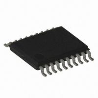
ATTINY167-15XD Atmel, ATTINY167-15XD Datasheet - Page 197

ATTINY167-15XD
Manufacturer Part Number
ATTINY167-15XD
Description
MCU AVR 16K FLASH 15MHZ 20-TSSOP
Manufacturer
Atmel
Series
AVR® ATtinyr
Datasheet
1.ATTINY167-15MD.pdf
(283 pages)
Specifications of ATTINY167-15XD
Core Processor
AVR
Core Size
8-Bit
Speed
16MHz
Connectivity
I²C, LIN, SPI, UART/USART, USI
Peripherals
Brown-out Detect/Reset, POR, PWM, Temp Sensor, WDT
Number Of I /o
16
Program Memory Size
16KB (8K x 16)
Program Memory Type
FLASH
Eeprom Size
512 x 8
Ram Size
512 x 8
Voltage - Supply (vcc/vdd)
2.7 V ~ 5.5 V
Data Converters
A/D 11x10b
Oscillator Type
Internal
Operating Temperature
-40°C ~ 150°C
Package / Case
20-TSSOP
Processor Series
ATTINY1x
Core
AVR8
Data Bus Width
8 bit
Data Ram Size
512 B
Maximum Clock Frequency
16 MHz
Maximum Operating Temperature
+ 85 C
Mounting Style
SMD/SMT
3rd Party Development Tools
EWAVR, EWAVR-BL
Development Tools By Supplier
ATAVRDRAGON, ATSTK500, ATSTK600, ATAVRISP2, ATAVRONEKIT
Minimum Operating Temperature
- 40 C
For Use With
ATSTK600-SOIC - STK600 SOCKET/ADAPTER FOR SOIC
Lead Free Status / RoHS Status
Lead free / RoHS Compliant
- Current page: 197 of 283
- Download datasheet (5Mb)
17.6
7728G–AVR–06/10
Changing Channel or Reference Selection
DC Clock
DSC
DIF
DCH
DCL
Figure 17-7. ADC Timing Diagram, Free Running Conversion
ycle Number
Table 17-1.
The MUX[4:0] and REFS[1:0] bits in the ADMUX register are single buffered through a tempo-
rary register to which the CPU has random access. This ensures that the channels and
reference selection only takes place at a safe point during the conversion. The channel and
reference selection is continuously updated until a conversion is started. Once the conversion
starts, the channel and reference selection is locked to ensure a sufficient sampling time for
the ADC. Continuous updating resumes in the last ADC clock cycle before the conversion
completes (ADIF in ADCSRA register is set). Note that the conversion starts on the following
rising ADC clock edge after ADSC is written. The user is thus advised not to write new channel
or reference selection values to ADMUX until one ADC clock cycle after ADSC is written.
If Auto Triggering is used, the exact time of the triggering event can be indeterministic. Special
care must be taken when updating the ADMUX register, in order to control which conversion
will be affected by the new settings.
If both ADATE and ADEN is written to one, an interrupt event can occur at any time. If the
ADMUX Register is changed in this period, the user cannot tell if the next conversion is based
on the old or the new settings. ADMUX can be safely updated in the following ways:
When updating ADMUX in one of these conditions, the new settings will affect the next ADC
conversion.
Condition
First conversion
Normal conversions
Auto Triggered conversions
Conversion
Complete
a. When ADATE or ADEN is cleared.
b. During conversion, minimum one ADC clock cycle after the trigger event.
c. After a conversion, before the Interrupt Flag used as trigger source is cleared.
One Conversion
11
12
ADC Conversion Time
13
Next Conversion
1
Sign and MSB of Result
LSB of Result
2
MUX and REFS
Update
3
Sample & Hold
4
(Cycles from Start of Conversion)
Sample & Hold
13.5 cycles
1.5 cycles
2 cycles
ATtiny87/ATtiny167
Conversion Time (Cycles)
13.5 cycles
25 cycles
13 cycles
197
Related parts for ATTINY167-15XD
Image
Part Number
Description
Manufacturer
Datasheet
Request
R

Part Number:
Description:
Manufacturer:
Atmel Corporation
Datasheet:

Part Number:
Description:
Manufacturer:
Atmel Corporation
Datasheet:

Part Number:
Description:
MCU AVR 16K FLASH 15MHZ 32-QFN
Manufacturer:
Atmel
Datasheet:

Part Number:
Description:
IC MCU AVR 16K FLASH 20TSSOP
Manufacturer:
Atmel
Datasheet:

Part Number:
Description:
MCU AVR 16K FLASH 15MHZ 32-QFN
Manufacturer:
Atmel
Datasheet:

Part Number:
Description:
MCU AVR 16K FLASH 15MHZ 20-SOIC
Manufacturer:
Atmel
Datasheet:

Part Number:
Description:
MCU AVR 16K FLASH 15MHZ 20-TSSOP
Manufacturer:
Atmel
Datasheet:

Part Number:
Description:
IC MCU AVR 16K FLASH 20SOIC
Manufacturer:
Atmel
Datasheet:


