ATTINY167-15XD Atmel, ATTINY167-15XD Datasheet - Page 199
ATTINY167-15XD
Manufacturer Part Number
ATTINY167-15XD
Description
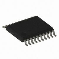
MCU AVR 16K FLASH 15MHZ 20-TSSOP
Manufacturer
Atmel
Series
AVR® ATtinyr
Datasheet
1.ATTINY167-15MD.pdf
(283 pages)
Specifications of ATTINY167-15XD
Core Processor
AVR
Core Size
8-Bit
Speed
16MHz
Connectivity
I²C, LIN, SPI, UART/USART, USI
Peripherals
Brown-out Detect/Reset, POR, PWM, Temp Sensor, WDT
Number Of I /o
16
Program Memory Size
16KB (8K x 16)
Program Memory Type
FLASH
Eeprom Size
512 x 8
Ram Size
512 x 8
Voltage - Supply (vcc/vdd)
2.7 V ~ 5.5 V
Data Converters
A/D 11x10b
Oscillator Type
Internal
Operating Temperature
-40°C ~ 150°C
Package / Case
20-TSSOP
Processor Series
ATTINY1x
Core
AVR8
Data Bus Width
8 bit
Data Ram Size
512 B
Maximum Clock Frequency
16 MHz
Maximum Operating Temperature
+ 85 C
Mounting Style
SMD/SMT
3rd Party Development Tools
EWAVR, EWAVR-BL
Development Tools By Supplier
ATAVRDRAGON, ATSTK500, ATSTK600, ATAVRISP2, ATAVRONEKIT
Minimum Operating Temperature
- 40 C
For Use With
ATSTK600-SOIC - STK600 SOCKET/ADAPTER FOR SOIC
Lead Free Status / RoHS Status
Lead free / RoHS Compliant


17.7.2
17.7.3
7728G–AVR–06/10
Analog Noise Canceling Techniques
ADC Accuracy Definitions
The ADC is optimized for analog signals with an output impedance of approximately 10 k or
less. If such a source is used, the sampling time will be negligible. If a source with higher
impedance is used, the sampling time will depend on how long time the source needs to
charge the S/H capacitor, with can vary widely. The user is recommended to only use low
impedant sources with slowly varying signals, since this minimizes the required charge trans-
fer to the S/H capacitor.
Signal components higher than the Nyquist frequency (f
distortion from unpredictable signal convolution. The user is advised to remove high frequency
components with a low-pass filter before applying the signals as inputs to the ADC.
Figure 17-8. Analog Input Circuitry
Digital circuitry inside and outside the device generates EMI which might affect the accuracy of
analog measurements. If conversion accuracy is critical, the noise level can be reduced by
applying the following techniques:
An n-bit single-ended ADC converts a voltage linearly between GND and V
(LSBs). The lowest code is read as 0, and the highest code is read as 2
Several parameters describe the deviation from the ideal behavior:
• Offset: The deviation of the first transition (0x000 to 0x001) compared to the ideal transition
(at 0.5 LSB). Ideal value: 0 LSB.
a. Keep analog signal paths as short as possible. Make sure analog tracks run over
b. Use the ADC noise canceler function to reduce induced noise from the CPU.
c. If any port pins are used as digital outputs, it is essential that these do not switch
the analog ground plane, and keep them well away from high-speed switching
digital tracks.
while a conversion is in progress.
ADCn
I
IH
I
IL
1..100 kO
ATtiny87/ATtiny167
ADC
C
/2) should not be present to avoid
S/H
= 14 pF
V
CC
/2
n
-1.
REF
in 2
n
steps
199
Related parts for ATTINY167-15XD
Image
Part Number
Description
Manufacturer
Datasheet
Request
R

Part Number:
Description:
Manufacturer:
Atmel Corporation
Datasheet:
Part Number:
Description:
Manufacturer:
Atmel Corporation
Datasheet:

Part Number:
Description:
MCU AVR 16K FLASH 15MHZ 32-QFN
Manufacturer:
Atmel
Datasheet:

Part Number:
Description:
IC MCU AVR 16K FLASH 20TSSOP
Manufacturer:
Atmel
Datasheet:
Part Number:
Description:
MCU AVR 16K FLASH 15MHZ 32-QFN
Manufacturer:
Atmel
Datasheet:

Part Number:
Description:
MCU AVR 16K FLASH 15MHZ 20-SOIC
Manufacturer:
Atmel
Datasheet:

Part Number:
Description:
MCU AVR 16K FLASH 15MHZ 20-TSSOP
Manufacturer:
Atmel
Datasheet:
Part Number:
Description:
IC MCU AVR 16K FLASH 20SOIC
Manufacturer:
Atmel
Datasheet: