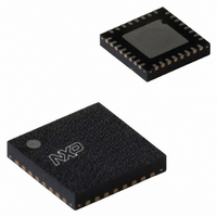
MFRC52301HN1,151 NXP Semiconductors, MFRC52301HN1,151 Datasheet - Page 26

MFRC52301HN1,151
Manufacturer Part Number
MFRC52301HN1,151
Description
IC MIFARE READER 32-HVQFN
Manufacturer
NXP Semiconductors
Series
MIFARE®r
Specifications of MFRC52301HN1,151
Frequency
13.56MHz
Package / Case
32-VQFN Exposed Pad, 32-HVQFN, 32-SQFN, 32-DHVQFN
Operating Current
7 mA
Operating Voltage
2.5 V to 3.6 V
Product
RFID Readers
Wireless Frequency
13.56 MHz
Interface Type
RS-232, I2C
Data Rate
100 Kbps
Operating Temperature Range
- 25 C to +85 C
Lead Free Status / RoHS Status
Lead free / RoHS Compliant
Features
-
Rf Type
-
Lead Free Status / RoHS Status
Lead free / RoHS Compliant
Other names
568-4766
935282956151
MFRC52301HN1
935282956151
MFRC52301HN1
NXP Semiconductors
MFRC523_32
Product data sheet
PUBLIC
8.4.3 Serial data switch
8.4.4 MFIN and MFOUT interface support
Two main blocks are implemented in the MFRC523. The digital block comprises the state
machines, encoder/decoder logic. The analog block comprises the modulator and
antenna drivers, the receiver and amplifiers. It is possible for the interface between these
two blocks to be configured so that the interfacing signals are routed to pins MFIN and
MFOUT.
This topology allows the analog block of the MFRC523 to be connected to the digital block
of another device.
The serial signal switch is controlled by the TxSelReg and RxSelReg registers.
Figure 20
The MFRC523 is divided into a digital circuit block and an analog circuit block. The digital
block contains state machines, encoder and decoder logic and so on. The analog block
contains the modulator and antenna drivers, receiver and amplifiers. The interface
between these two blocks can be configured so that the interfacing signals can be routed
to pins MFIN and MFOUT; see
using TxSelReg register’s MFOutSel[3:0] and DriverSel[1:0] bits and RxSelReg register’s
UARTSel[1:0] bits.
This topology allows some parts of the analog block to be connected to the digital block of
another device.
Switch MFOutSel in the TxSelReg register can be used to measure MIFARE and
ISO/IEC14443 A related signals. This is especially important during the design-in phase
or for test purposes as it enables checking of the transmitted and received data.
The most important use of pins MFIN and MFOUT is found in the active antenna concept.
An external active antenna circuit can be connected to the MFRC523’s digital block.
Switch MFOutSel must be configured so that the internal Miller encoded signal is sent to
pin MFOUT (MFOutSel = 100b). UARTSel[1:0] must be configured to receive a
Manchester signal with subcarrier from pin MFIN (UARTSel[1:0] = 01).
It is possible to connect a passive antenna to pins TX1, TX2 and RX (using the
appropriate filter and matching circuit) and an active antenna to pins MFOUT and MFIN at
the same time. In this configuration, two RF circuits can be driven (one after another) by a
single host processor.
Fig 20. Serial data switch for TX1 and TX2
shows the serial data switch for TX1 and TX2.
INTERNAL
CODER
MFIN
Rev. 3.2 — 12 January 2010
PolMFin = 0
InvMod = 1
INVERT IF
INVERT IF
115232
Figure 21 on page
envelope
3-state
1
DriverSel[1:0]
27. This configuration is implemented
00
01
10
11
to driver TX1 and TX2
0 = impedance = modulated
1 = impedance = CW
Contactless reader IC
MFRC523
© NXP B.V. 2010. All rights reserved.
001aak593
26 of 98


