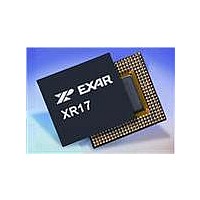
XR17V258IV-F Exar Corporation, XR17V258IV-F Datasheet - Page 29

XR17V258IV-F
Manufacturer Part Number
XR17V258IV-F
Description
IC UART PCI BUS OCTAL 144LQFP
Manufacturer
Exar Corporation
Type
Octal UARTr
Datasheet
1.XR17V258IVTR-F.pdf
(69 pages)
Specifications of XR17V258IV-F
Number Of Channels
8
Package / Case
144-LQFP
Features
*
Fifo's
64 Byte
Protocol
RS485
Voltage - Supply
3.3V, 5V
With Auto Flow Control
Yes
With Irda Encoder/decoder
Yes
With False Start Bit Detection
Yes
With Modem Control
Yes
Mounting Type
Surface Mount
Data Rate
8 Mbps
Supply Voltage (max)
3.6 V
Supply Voltage (min)
3 V
Supply Current
4 mA
Maximum Operating Temperature
+ 85 C
Minimum Operating Temperature
- 45 C
Mounting Style
SMD/SMT
Operating Supply Voltage
3 V to 3.6 V
No. Of Channels
8
Uart Features
Tx/Rx FIFO Counters
Supply Voltage Range
3V To 3.6V
Operating Temperature Range
-40°C To +85°C
Digital Ic Case Style
LQFP
No. Of Pins
144
Rohs Compliant
Yes
Lead Free Status / RoHS Status
Lead free / RoHS Compliant
Lead Free Status / RoHS Status
Lead free / RoHS Compliant, Lead free / RoHS Compliant
Available stocks
Company
Part Number
Manufacturer
Quantity
Price
Company:
Part Number:
XR17V258IV-F
Manufacturer:
EXAR
Quantity:
295
Company:
Part Number:
XR17V258IV-F
Manufacturer:
Exar Corporation
Quantity:
10 000
Part Number:
XR17V258IV-F
Manufacturer:
EXAR/艾科嘉
Quantity:
20 000
REV. 1.0.2
(channel 2),......., 0xF00 (channel 7). This operation is at least 16 times faster than reading the data in 64
separate 8-bit memory reads of RHR register (0x000 for channel 0, 0x200 for channel 1, 0x400 for channel
2,......, 0xE00 for channel 7).
The XR17V258 also provides the same RX FIFO data along with the LSR status information of each byte side-
by-side, at locations 0x180 (channel 0), 0x380 (channel 1), 0x580 (channel 2), ....., 0xF80 (channel 3). The
entire RX data along with the status can be downloaded in a single PCI Burst Read operation of 32 DWORD
reads. The Status and Data bytes must be read in 16 or 32 bits format to maintain data integrity. The following
tables show this clearly.
3.1.2
Data Bit-31
WITH N
Data Bit-31
WITH LSR
Read n+0 to n+3
Read n+4 to n+7
Read n+0 to n+1
Read n+2 to n+3
PCI Bus
R
R
PCI Bus
EAD
EAD
B7 B6 B5 B4 B3 B2 B1 B0
B7 B6 B5 B4 B3 B2 B1 B0
Etc.
Receive Data Byte n+1
RX FIFO,
RX FIFO,
Etc
Receive Data Byte n+3
O
Special Rx FIFO Data Unloading at locations 0x180, 0x380, 0x580, and 0x780
E
E
RRORS
RRORS
Channel 0 to 7 Receive Data with Line Status Register in a 32-bit alignment through the Configuration
Channel 0 to 7 ReceiveData in 32-bit alignment through the Configuration Register Address
Register Address 0x0180, 0x0380, 0x0580, 0x0780, 0x0980, 0x0B80, 0x0D80 and 0x0F80
FIFO Data n+3
FIFO Data n+7
FIFO Data n+1
FIFO Data n+3
B
B
0x0100, 0x0300, 0x0500, 0x0700, 0x0900, 0x0B00, 0x0D00 and 0x0F00
B7 B6 B5 B4 B3 B2 B1 B0
B7 B6 B5 B4 B3 B2 B1 B0
YTE
YTE
66MHZ PCI BUS OCTAL UART WITH POWER MANAGEMENT SUPPORT
Line Status Register n+1
Receive Data Byte n+2
3
3
FIFO Data n+2
FIFO Data n+6
LSR n+1
LSR n+3
B
B
YTE
YTE
29
B7 B6 B5 B4 B3 B2 B1 B0
B7 B6 B5 B4 B3 B2 B1 B0
2
2
Receive Data Byte n+1
Receive Data Byte n+0
FIFO Data n+1
FIFO Data n+5
FIFO Data n+0
FIFO Data n+2
B
B
YTE
YTE
1
1
B7 B6 B5 B4 B3 B2 B1 B0
B7 B6 B5 B4 B3 B2 B1 B0
Receive Data Byte n+0
Line Status Register n+0
FIFO Data n+0
FIFO Data n+4
XR17V258
LSR n+0
LSR n+2
B
B
YTE
YTE
Data Bit-0
PCI Bus
0
0
Data Bit-0
PCI Bus


