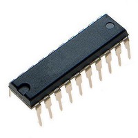
ATTINY461-20PU Atmel, ATTINY461-20PU Datasheet - Page 115

ATTINY461-20PU
Manufacturer Part Number
ATTINY461-20PU
Description
Microcontrollers (MCU) 4kB Flash 0.256kB EEPROM 16 I/O Pins
Manufacturer
Atmel
Specifications of ATTINY461-20PU
Processor Series
ATTINY4x
Core
AVR8
Data Bus Width
8 bit
Data Ram Size
256 B
Interface Type
2-Wire/SPI/USI
Maximum Clock Frequency
20 MHz
Number Of Programmable I/os
16
Number Of Timers
2
Operating Supply Voltage
4.5 V to 5.5 V
Maximum Operating Temperature
+ 85 C
Mounting Style
Through Hole
3rd Party Development Tools
EWAVR, EWAVR-BL
Development Tools By Supplier
ATAVRDRAGON, ATSTK500, ATSTK600, ATAVRISP2, ATAVRONEKIT
Minimum Operating Temperature
- 40 C
On-chip Adc
11-ch x 10-bit
Program Memory Type
Flash
Program Memory Size
4 KB
Package / Case
PDIP-20
Package
20PDIP
Device Core
AVR
Family Name
ATtiny
Maximum Speed
20 MHz
Ram Size
256 Byte
Operating Temperature
-40 to 85 °C
Lead Free Status / RoHS Status
Lead free / RoHS Compliant
- Current page: 115 of 242
- Download datasheet (5Mb)
12.12.2
2588E–AVR–08/10
TCCR1B – Timer/Counter1 Control Register B
COM1B1S and COM1B0S in TCCR1C will show here. See
Register C” on page
• Bit 3 – FOC1A: Force Output Compare Match 1A
The FOC1A bit is only active when the PWM1A bit specify a non-PWM mode.
Writing a logical one to this bit forces a change in the Waveform Output (OCW1A) and the Out-
put Compare pin (OC1A) according to the values already set in COM1A1 and COM1A0. If
COM1A1 and COM1A0 written in the same cycle as FOC1A, the new settings will be used. The
Force Output Compare bit can be used to change the output pin value regardless of the timer
value. The automatic action programmed in COM1A1 and COM1A0 takes place as if a compare
match had occurred, but no interrupt is generated.
The FOC1A bit always reads zero.
• Bit 2 – FOC1B: Force Output Compare Match 1B
The FOC1B bit is only active when the PWM1B bit specify a non-PWM mode.
Writing a logical one to this bit forces a change in the Waveform Output (OCW1B) and the Out-
put Compare pin (OC1B) according to the values already set in COM1B1 and COM1B0. If
COM1B1 and COM1B0 written in the same cycle as FOC1B, the new settings will be used. The
Force Output Compare bit can be used to change the output pin value regardless of the timer
value. The automatic action programmed in COM1B1 and COM1B0 takes place as if a compare
match had occurred, but no interrupt is generated.
The FOC1B bit always reads zero.
• Bit 1 – PWM1A: Pulse Width Modulator A Enable
When set (one) this bit enables PWM mode based on comparator OCR1A
• Bit 0 – PWM1B: Pulse Width Modulator B Enable
When set (one) this bit enables PWM mode based on comparator OCR1B.
• Bit 7 – PWM1X : PWM Inversion Mode
When this bit is set (one), the PWM Inversion Mode is selected and the Dead Time Generator
outputs, OC1x and OC1x are inverted.
• Bit 6 – PSR1 : Prescaler Reset Timer/Counter1
When this bit is set (one), the Timer/Counter1 prescaler (TCNT1 is unaffected) will be reset. The
bit will be cleared by hardware after the operation is performed. Writing a zero to this bit will have
no effect. This bit will always read as zero.
• Bits 5,4 – DTPS11, DTPS10: Dead Time Prescaler Bits
The Timer/Counter1 Control Register B is a 8-bit read/write register.
Bit
0x2F (0x4F)
Read/Write
Initial value
PWM1X
R/W
7
0
117.
PSR1
R/W
6
0
DTPS11
R/W
5
0
DTPS10
R/W
4
0
CS13
R/W
3
0
“TCCR1C – Timer/Counter1 Control
CS12
R/W
2
0
CS11
R/W
1
0
CS10
R/W
0
0
TCCR1B
115
Related parts for ATTINY461-20PU
Image
Part Number
Description
Manufacturer
Datasheet
Request
R

Part Number:
Description:
Manufacturer:
Atmel Corporation
Datasheet:

Part Number:
Description:
Manufacturer:
Atmel Corporation
Datasheet:

Part Number:
Description:
IC AVR MCU 4K 20MHZ 32-QFN
Manufacturer:
Atmel
Datasheet:

Part Number:
Description:
IC MCU AVR 4K FLASH 20MHZ 20SOIC
Manufacturer:
Atmel
Datasheet:

Part Number:
Description:
MCU AVR 4K FLASH 15MHZ 32-QFN
Manufacturer:
Atmel
Datasheet:

Part Number:
Description:
MCU AVR 4KB FLASH 15MHZ 32-VQFN
Manufacturer:
Atmel
Datasheet:

Part Number:
Description:
MCU AVR 4KB FLASH 20MHZ 20SOIC
Manufacturer:
Atmel
Datasheet:

Part Number:
Description:
IC MCU AVR 4K 20MHZ 32QFN
Manufacturer:
Atmel
Datasheet:

Part Number:
Description:
IC, MCU, 8BIT, 2K FLASH, 20SOIC
Manufacturer:
Atmel
Datasheet:

Part Number:
Description:
IC, MCU, 8BIT, 2K FLASH, 20PDIP
Manufacturer:
Atmel
Datasheet:


