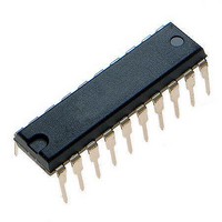
ATTINY461-20PU Atmel, ATTINY461-20PU Datasheet - Page 63

ATTINY461-20PU
Manufacturer Part Number
ATTINY461-20PU
Description
Microcontrollers (MCU) 4kB Flash 0.256kB EEPROM 16 I/O Pins
Manufacturer
Atmel
Specifications of ATTINY461-20PU
Processor Series
ATTINY4x
Core
AVR8
Data Bus Width
8 bit
Data Ram Size
256 B
Interface Type
2-Wire/SPI/USI
Maximum Clock Frequency
20 MHz
Number Of Programmable I/os
16
Number Of Timers
2
Operating Supply Voltage
4.5 V to 5.5 V
Maximum Operating Temperature
+ 85 C
Mounting Style
Through Hole
3rd Party Development Tools
EWAVR, EWAVR-BL
Development Tools By Supplier
ATAVRDRAGON, ATSTK500, ATSTK600, ATAVRISP2, ATAVRONEKIT
Minimum Operating Temperature
- 40 C
On-chip Adc
11-ch x 10-bit
Program Memory Type
Flash
Program Memory Size
4 KB
Package / Case
PDIP-20
Package
20PDIP
Device Core
AVR
Family Name
ATtiny
Maximum Speed
20 MHz
Ram Size
256 Byte
Operating Temperature
-40 to 85 °C
Lead Free Status / RoHS Status
Lead free / RoHS Compliant
- Current page: 63 of 242
- Download datasheet (5Mb)
10.2.1
2588E–AVR–08/10
Alternate Functions of Port A
The Port A pins with alternate function are shown in
Table 10-3.
• Port A, Bit 7 – ADC6/AIN0/PCINT7
• Port A, Bit 6 – ADC5/AIN1/PCINT6
• ADC6: Analog to Digital Converter, Channel 6
• AIN0: Analog Comparator Input. Configure the port pin as input with the internal pull-up
• PCINT7: Pin Change Interrupt source 8.
• ADC5: Analog to Digital Converter, Channel 5.
• AIN1: Analog Comparator Input. Configure the port pin as input with the internal pull-up
• PCINT6: Pin Change Interrupt source 6.
switched off to avoid the digital port function from interfering with the function of the Analog
Comparator.
switched off to avoid the digital port function from interfering with the function of the Analog
Comparator.
Port Pin
PA7
PA6
PA5
PA4
PA3
PA2
PA1
PA0
Port B Pins Alternate Functions
Alternate Function
ADC6:
AIN0:
PCINT7: Pin Change Interrupt 0, Source 7
ADC5:
AIN1:
PCINT6: Pin Change Interrupt 0, Source 6
ADC4:
AIN2:
PCINT5: Pin Change Interrupt 0, Source 5
ADC3:
ICP0:
PCINT4: Pin Change Interrupt 0, Source 4
AREF:
PCINT3: Pin Change Interrupt 0, Source 3
ADC2:
INT1:
USCK: USI Clock (Three Wire Mode)
SCL :
PCINT2: Pin Change Interrupt 0, Source 2
ADC1:
DO:
PCINT1:Pin Change Interrupt 0, Source 1
ADC0:
DI:
SDA:
PCINT0: Pin Change Interrupt 0, Source 0
ADC Input Channel 6
Analog Comparator Input
ADC Input Channel 5
Analog Comparator Input
ADC Input Channel 4
Analog Comparator Input
ADC Input Channel 3
Timer/Counter0 Input Capture Pin
External Analog Reference
ADC Input Channel 2
External Interrupt 1 Input
USI Clock (Two Wire Mode)
ADC Input Channel 1
USI Data Output (Three Wire Mode)
ADC Input Channel 0
USI Data Input (Three Wire Mode)
USI Data Input (Two Wire Mode)
.
Table
10-3.
63
Related parts for ATTINY461-20PU
Image
Part Number
Description
Manufacturer
Datasheet
Request
R

Part Number:
Description:
Manufacturer:
Atmel Corporation
Datasheet:

Part Number:
Description:
Manufacturer:
Atmel Corporation
Datasheet:

Part Number:
Description:
IC AVR MCU 4K 20MHZ 32-QFN
Manufacturer:
Atmel
Datasheet:

Part Number:
Description:
IC MCU AVR 4K FLASH 20MHZ 20SOIC
Manufacturer:
Atmel
Datasheet:

Part Number:
Description:
MCU AVR 4K FLASH 15MHZ 32-QFN
Manufacturer:
Atmel
Datasheet:

Part Number:
Description:
MCU AVR 4KB FLASH 15MHZ 32-VQFN
Manufacturer:
Atmel
Datasheet:

Part Number:
Description:
MCU AVR 4KB FLASH 20MHZ 20SOIC
Manufacturer:
Atmel
Datasheet:

Part Number:
Description:
IC MCU AVR 4K 20MHZ 32QFN
Manufacturer:
Atmel
Datasheet:

Part Number:
Description:
IC, MCU, 8BIT, 2K FLASH, 20SOIC
Manufacturer:
Atmel
Datasheet:

Part Number:
Description:
IC, MCU, 8BIT, 2K FLASH, 20PDIP
Manufacturer:
Atmel
Datasheet:


