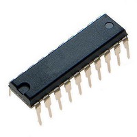
ATTINY461-20PU Atmel, ATTINY461-20PU Datasheet - Page 25

ATTINY461-20PU
Manufacturer Part Number
ATTINY461-20PU
Description
Microcontrollers (MCU) 4kB Flash 0.256kB EEPROM 16 I/O Pins
Manufacturer
Atmel
Specifications of ATTINY461-20PU
Processor Series
ATTINY4x
Core
AVR8
Data Bus Width
8 bit
Data Ram Size
256 B
Interface Type
2-Wire/SPI/USI
Maximum Clock Frequency
20 MHz
Number Of Programmable I/os
16
Number Of Timers
2
Operating Supply Voltage
4.5 V to 5.5 V
Maximum Operating Temperature
+ 85 C
Mounting Style
Through Hole
3rd Party Development Tools
EWAVR, EWAVR-BL
Development Tools By Supplier
ATAVRDRAGON, ATSTK500, ATSTK600, ATAVRISP2, ATAVRONEKIT
Minimum Operating Temperature
- 40 C
On-chip Adc
11-ch x 10-bit
Program Memory Type
Flash
Program Memory Size
4 KB
Package / Case
PDIP-20
Package
20PDIP
Device Core
AVR
Family Name
ATtiny
Maximum Speed
20 MHz
Ram Size
256 Byte
Operating Temperature
-40 to 85 °C
Lead Free Status / RoHS Status
Lead free / RoHS Compliant
- Current page: 25 of 242
- Download datasheet (5Mb)
6.1.3
6.1.4
6.1.5
6.1.6
6.2
2588E–AVR–08/10
Clock Sources
Flash Clock – clk
ADC Clock – clk
Fast Peripheral Clock – clk
PLL System Clock – clk
The Flash clock controls operation of the Flash interface. The Flash clock is usually active simul-
taneously with the CPU clock.
The ADC is provided with a dedicated clock domain. This allows halting the CPU and I/O clocks
in order to reduce noise generated by digital circuitry. This gives more accurate ADC conversion
results.
Selected peripherals can be clocked at a frequency higher than the CPU core. The fast periph-
eral clock is generated by an on-chip PLL circuit.
The PLL can also be used to generate a system clock. The clock signal can be prescaled to
avoid overclocking the CPU.
The device has the following clock source options, selectable by Flash Fuse bits as shown
below. The clock from the selected source is input to the AVR clock generator, and routed to the
appropriate modules.
Table 6-1.
Note:
The various choices for each clocking option is given in the following sections. When the CPU
wakes up from Power-down or Power-save, the selected clock source is used to time the start-
up, ensuring stable oscillator operation before instruction execution starts. When the CPU starts
from reset, there is an additional delay allowing the power to reach a stable level before com-
ADC
Device Clocking Option
External Clock (see
High-Frequency PLL Clock (see
Calibrated Internal 8 MHz Oscillator (see
Internal 128 kHz Oscillator (see
Low-Frequency Crystal Oscillator (see
Crystal Oscillator / Ceramic Resonator
0.4...0.9 MHz (see
Crystal Oscillator / Ceramic Resonator
0.9...3.0 MHz (see
Crystal Oscillator / Ceramic Resonator
3...8 MHz (see
Crystal Oscillator / Ceramic Resonator
8...20 MHz (see
FLASH
1. For all fuses “1” means unprogrammed and “0” means programmed.
ADC
PCK
Device Clocking Options Select
page
page
page
page
page
30)
30)
30)
30)
26)
page
page
29)
26)
page
page
29)
28)
(1)
vs. PB4 and PB5 Functionality
CKSEL3:0
0000
0001
0010
0011
1000
1001
1010
1011
1100
1101
01xx
1110
1111
XTAL1
XTAL1
XTAL1
XTAL1
XTAL1
XTAL1
PB4
I/O
I/O
I/O
XTAL2
XTAL2
XTAL2
XTAL2
XTAL2
PB5
I/O
I/O
I/O
I/O
25
Related parts for ATTINY461-20PU
Image
Part Number
Description
Manufacturer
Datasheet
Request
R

Part Number:
Description:
Manufacturer:
Atmel Corporation
Datasheet:

Part Number:
Description:
Manufacturer:
Atmel Corporation
Datasheet:

Part Number:
Description:
IC AVR MCU 4K 20MHZ 32-QFN
Manufacturer:
Atmel
Datasheet:

Part Number:
Description:
IC MCU AVR 4K FLASH 20MHZ 20SOIC
Manufacturer:
Atmel
Datasheet:

Part Number:
Description:
MCU AVR 4K FLASH 15MHZ 32-QFN
Manufacturer:
Atmel
Datasheet:

Part Number:
Description:
MCU AVR 4KB FLASH 15MHZ 32-VQFN
Manufacturer:
Atmel
Datasheet:

Part Number:
Description:
MCU AVR 4KB FLASH 20MHZ 20SOIC
Manufacturer:
Atmel
Datasheet:

Part Number:
Description:
IC MCU AVR 4K 20MHZ 32QFN
Manufacturer:
Atmel
Datasheet:

Part Number:
Description:
IC, MCU, 8BIT, 2K FLASH, 20SOIC
Manufacturer:
Atmel
Datasheet:

Part Number:
Description:
IC, MCU, 8BIT, 2K FLASH, 20PDIP
Manufacturer:
Atmel
Datasheet:


