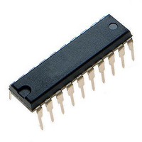
ATTINY461-20PU Atmel, ATTINY461-20PU Datasheet - Page 99

ATTINY461-20PU
Manufacturer Part Number
ATTINY461-20PU
Description
Microcontrollers (MCU) 4kB Flash 0.256kB EEPROM 16 I/O Pins
Manufacturer
Atmel
Specifications of ATTINY461-20PU
Processor Series
ATTINY4x
Core
AVR8
Data Bus Width
8 bit
Data Ram Size
256 B
Interface Type
2-Wire/SPI/USI
Maximum Clock Frequency
20 MHz
Number Of Programmable I/os
16
Number Of Timers
2
Operating Supply Voltage
4.5 V to 5.5 V
Maximum Operating Temperature
+ 85 C
Mounting Style
Through Hole
3rd Party Development Tools
EWAVR, EWAVR-BL
Development Tools By Supplier
ATAVRDRAGON, ATSTK500, ATSTK600, ATAVRISP2, ATAVRONEKIT
Minimum Operating Temperature
- 40 C
On-chip Adc
11-ch x 10-bit
Program Memory Type
Flash
Program Memory Size
4 KB
Package / Case
PDIP-20
Package
20PDIP
Device Core
AVR
Family Name
ATtiny
Maximum Speed
20 MHz
Ram Size
256 Byte
Operating Temperature
-40 to 85 °C
Lead Free Status / RoHS Status
Lead free / RoHS Compliant
- Current page: 99 of 242
- Download datasheet (5Mb)
12.7.1
12.8
12.8.1
2588E–AVR–08/10
Modes of Operation
Compare Output Mode and Waveform Generation
Normal Mode
The design of the Output Compare Pin Configuration logic allows initialization of the OC1x state
before the output is enabled. Note that some COM1x1:0 bit settings are reserved for certain
modes of operation. For Output Compare Pin Configurations refer to
Table 12-3 on page
105, and
The Waveform Generator uses the COM1x1:0 bits differently in Normal mode and PWM modes.
For all modes, setting the COM1x1:0 = 0 tells the Waveform Generator that no action on the
OCW1x Output is to be performed on the next Compare Match. For compare output actions in
the non-PWM modes refer to
on page
A change of the COM1x1:0 bits state will have effect at the first Compare Match after the bits are
written. For non-PWM modes, the action can be forced to have immediate effect by using the
FOC1x strobe bits.
The mode of operation, i.e., the behavior of the Timer/Counter and the Output Compare pins, is
defined by the combination of waveform generation mode bits (PWM1A, PWM1B, and
WGM11:10) and compare output mode bits (COM1x1:0). The Compare Output mode bits do not
affect the counting sequence, while the Waveform Generation mode bits do. The COM1x1:0 bits
control whether the PWM output generated should be inverted, non-inverted or complementary.
For non-PWM modes the COM1x1:0 bits control whether the output should be set, cleared, or
toggled at a Compare Match.
The simplest mode of operation is Normal mode (PWM1A/PWM1B = 0), where the counter
counts from BOTTOM to TOP (defined as OCR1C) then restarts from BOTTOM. The OCR1C
defines the TOP value for the counter, hence also its resolution, and allows control of the Com-
pare Match output frequency. In toggle Compare Output Mode the Waveform Output (OCW1x)
is toggled at Compare Match between TCNT1 and OCR1x. In non-inverting Compare Output
Mode the Waveform Output is cleared on the Compare Match. In inverting Compare Output
Mode the Waveform Output is set on Compare Match. The timing diagram for Normal mode is
shown in
Figure 12-11. Normal Mode, Timing Diagram
OCWnx
(COMnx=1)
TCNTn
Period
112, and for the Phase and Frequency Correct PWM refer to
Table 12-7 on page
Figure
12-11.
102,
1
Table 12-4 on page
106.
Table 12-8 on page
2
104,
3
112. For fast PWM mode, refer to
Table 12-5 on page
4
Table 12-10 on page
Table 12-2 on page
105,
TOVn Interrupt Flag Set
OCnx Interrupt Flag Set
Table 12-6 on page
Table 12-9
100,
113.
99
Related parts for ATTINY461-20PU
Image
Part Number
Description
Manufacturer
Datasheet
Request
R

Part Number:
Description:
Manufacturer:
Atmel Corporation
Datasheet:

Part Number:
Description:
Manufacturer:
Atmel Corporation
Datasheet:

Part Number:
Description:
IC AVR MCU 4K 20MHZ 32-QFN
Manufacturer:
Atmel
Datasheet:

Part Number:
Description:
IC MCU AVR 4K FLASH 20MHZ 20SOIC
Manufacturer:
Atmel
Datasheet:

Part Number:
Description:
MCU AVR 4K FLASH 15MHZ 32-QFN
Manufacturer:
Atmel
Datasheet:

Part Number:
Description:
MCU AVR 4KB FLASH 15MHZ 32-VQFN
Manufacturer:
Atmel
Datasheet:

Part Number:
Description:
MCU AVR 4KB FLASH 20MHZ 20SOIC
Manufacturer:
Atmel
Datasheet:

Part Number:
Description:
IC MCU AVR 4K 20MHZ 32QFN
Manufacturer:
Atmel
Datasheet:

Part Number:
Description:
IC, MCU, 8BIT, 2K FLASH, 20SOIC
Manufacturer:
Atmel
Datasheet:

Part Number:
Description:
IC, MCU, 8BIT, 2K FLASH, 20PDIP
Manufacturer:
Atmel
Datasheet:


