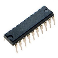
ATTINY461-20PU Atmel, ATTINY461-20PU Datasheet - Page 127

ATTINY461-20PU
Manufacturer Part Number
ATTINY461-20PU
Description
Microcontrollers (MCU) 4kB Flash 0.256kB EEPROM 16 I/O Pins
Manufacturer
Atmel
Specifications of ATTINY461-20PU
Processor Series
ATTINY4x
Core
AVR8
Data Bus Width
8 bit
Data Ram Size
256 B
Interface Type
2-Wire/SPI/USI
Maximum Clock Frequency
20 MHz
Number Of Programmable I/os
16
Number Of Timers
2
Operating Supply Voltage
4.5 V to 5.5 V
Maximum Operating Temperature
+ 85 C
Mounting Style
Through Hole
3rd Party Development Tools
EWAVR, EWAVR-BL
Development Tools By Supplier
ATAVRDRAGON, ATSTK500, ATSTK600, ATAVRISP2, ATAVRONEKIT
Minimum Operating Temperature
- 40 C
On-chip Adc
11-ch x 10-bit
Program Memory Type
Flash
Program Memory Size
4 KB
Package / Case
PDIP-20
Package
20PDIP
Device Core
AVR
Family Name
ATtiny
Maximum Speed
20 MHz
Ram Size
256 Byte
Operating Temperature
-40 to 85 °C
Lead Free Status / RoHS Status
Lead free / RoHS Compliant
- Current page: 127 of 242
- Download datasheet (5Mb)
13.3.2
2588E–AVR–08/10
SPI Master Operation Example
Figure 13-3. Three-wire Mode, Timing Diagram
The Three-wire mode timing is shown in Figure 13-3. At the top of the figure is a USCK cycle ref-
erence. One bit is shifted into the USI Data Register (USIDR) for each of these cycles. The
USCK timing is shown for both external clock modes. In External Clock mode 0 (USICS0 = 0), DI
is sampled at positive edges, and DO is changed (Data Register is shifted by one) at negative
edges. In external clock mode 1 (USICS0 = 1) the opposite edges with respect to mode 0 are
used. In other words, data is sampled at negative and output is changed at positive edges. The
USI clock modes corresponds to the SPI data mode 0 and 1.
Referring to the timing diagram
The following code demonstrates how to use the USI module as a SPI Master:
CYCLE
1. The slave and master devices set up their data outputs and, depending on the protocol
2. The master software generates a clock pulse by toggling the USCK line twice (C and
3. Step 2. is repeated eight times for a complete register (byte) transfer.
4. After eight clock pulses (i.e., 16 clock edges) the counter will overflow and indicate that
USCK
USCK
SPITransfer:
DO
DI
used, enable their output drivers (mark A and B). The output is set up by writing the
data to be transmitted to the USI Data Register. The output is enabled by setting the
corresponding bit in the Data Direction Register of Port A. Note that there is not a pre-
ferred order of points A and B in the figure, but both must be at least one half USCK
cycle before point C, where the data is sampled. This is in order to ensure that the data
setup requirement is satisfied. The 4-bit counter is reset to zero.
D). The bit values on the data input (DI) pins are sampled by the USI on the first edge
(C), and the data output is changed on the opposite edge (D). The 4-bit counter will
count both edges.
the transfer has been completed. The data bytes transferred must now be processed
before a new transfer can be initiated. The overflow interrupt will wake up the processor
if it is set to Idle mode. Depending on the protocol used the slave device can now set its
output to high impedance.
sts
ldi
sts
ldi
( Reference )
A
USIDR,r16
r16,(1<<USIOIF)
USISR,r16
r16,(1<<USIWM0)|(1<<USICS1)|(1<<USICLK)|(1<<USITC)
B
MSB
MSB
C
1
D
2
6
6
(Figure
3
5
5
13-3), a bus transfer involves the following steps:
4
4
4
5
3
3
6
2
2
7
1
1
LSB
LSB
8
E
127
Related parts for ATTINY461-20PU
Image
Part Number
Description
Manufacturer
Datasheet
Request
R

Part Number:
Description:
Manufacturer:
Atmel Corporation
Datasheet:

Part Number:
Description:
Manufacturer:
Atmel Corporation
Datasheet:

Part Number:
Description:
IC AVR MCU 4K 20MHZ 32-QFN
Manufacturer:
Atmel
Datasheet:

Part Number:
Description:
IC MCU AVR 4K FLASH 20MHZ 20SOIC
Manufacturer:
Atmel
Datasheet:

Part Number:
Description:
MCU AVR 4K FLASH 15MHZ 32-QFN
Manufacturer:
Atmel
Datasheet:

Part Number:
Description:
MCU AVR 4KB FLASH 15MHZ 32-VQFN
Manufacturer:
Atmel
Datasheet:

Part Number:
Description:
MCU AVR 4KB FLASH 20MHZ 20SOIC
Manufacturer:
Atmel
Datasheet:

Part Number:
Description:
IC MCU AVR 4K 20MHZ 32QFN
Manufacturer:
Atmel
Datasheet:

Part Number:
Description:
IC, MCU, 8BIT, 2K FLASH, 20SOIC
Manufacturer:
Atmel
Datasheet:

Part Number:
Description:
IC, MCU, 8BIT, 2K FLASH, 20PDIP
Manufacturer:
Atmel
Datasheet:


