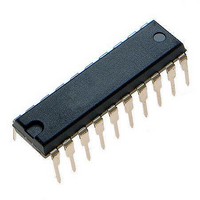
ATTINY461-20PU Atmel, ATTINY461-20PU Datasheet - Page 155

ATTINY461-20PU
Manufacturer Part Number
ATTINY461-20PU
Description
Microcontrollers (MCU) 4kB Flash 0.256kB EEPROM 16 I/O Pins
Manufacturer
Atmel
Specifications of ATTINY461-20PU
Processor Series
ATTINY4x
Core
AVR8
Data Bus Width
8 bit
Data Ram Size
256 B
Interface Type
2-Wire/SPI/USI
Maximum Clock Frequency
20 MHz
Number Of Programmable I/os
16
Number Of Timers
2
Operating Supply Voltage
4.5 V to 5.5 V
Maximum Operating Temperature
+ 85 C
Mounting Style
Through Hole
3rd Party Development Tools
EWAVR, EWAVR-BL
Development Tools By Supplier
ATAVRDRAGON, ATSTK500, ATSTK600, ATAVRISP2, ATAVRONEKIT
Minimum Operating Temperature
- 40 C
On-chip Adc
11-ch x 10-bit
Program Memory Type
Flash
Program Memory Size
4 KB
Package / Case
PDIP-20
Package
20PDIP
Device Core
AVR
Family Name
ATtiny
Maximum Speed
20 MHz
Ram Size
256 Byte
Operating Temperature
-40 to 85 °C
Lead Free Status / RoHS Status
Lead free / RoHS Compliant
- Current page: 155 of 242
- Download datasheet (5Mb)
15.13 Register Description
15.13.1
2588E–AVR–08/10
ADMUX – ADC Multiplexer Selection Register
assuming calibration at room temperature. Better accuracies are achieved by using two
temperature points for calibration.
Table 15-2.
The values described in
temperature sensor output voltage varies from one chip to another. To be capable of achieving
more accurate results the temperature measurement can be calibrated in the application soft-
ware. The sofware calibration can be done using the formula:
where ADCH and ADCL are the ADC data registers, k is the fixed slope coefficient and T
the temperature sensor offset. Typically, k is very close to 1.0 and in single-point calibration the
coefficient may be omitted. Where higher accuracy is required the slope coefficient should be
evaluated based on measurements at two temperatures.
• Bits 7:6 – REFS1:REFS0: Voltage Reference Selection Bits
These bits together with the REFS2 bit from the ADC Control and Status Register B (ADCSRB)
select the voltage reference for the ADC, as shown in
Table 15-3.
If these bits are changed during a conversion, the change will not go in effect until this conver-
sion is complete (ADIF in ADCSR is set). Also note, that when these bits are changed, the next
conversion will take 25 ADC clock cycles.
Bit
0x07 (0x27)
Read/Write
Initial Value
Temperature
ADC
T = k * [(ADCH << 8) | ADCL] + T
REFS2
X
X
0
0
1
1
Temperature vs. Sensor Output Voltage (Typical Case)
Voltage Reference Selections for ADC
REFS1
R/W
7
0
REFS1
0
0
1
1
1
1
REFS0
Table 15-2
R/W
6
0
230 LSB
-40 °C
ADLAR
REFS0
R/W
5
0
0
1
0
1
0
1
are typical values. However, due to process variation the
MUX4
OS
R/W
4
0
Voltage Reference Selection
V
disconnected from AREF
External voltage reference at AREF pin,
internal voltage reference turned off
Internal 1.1V voltage reference
Reserved
Internal 2.56V voltage reference,
without external bypass capacitor,
disconnected from AREF
Internal 2.56V voltage reference,
with external bypass capacitor at AREF pin
CC
used as voltage reference,
MUX3
R/W
3
0
Table
300 LSB
+25 °C
15-3.
MUX2
R/W
2
0
MUX1
R/W
1
0
MUX0
R/W
0
0
370 LSB
+85 °C
ADMUX
OS
155
is
Related parts for ATTINY461-20PU
Image
Part Number
Description
Manufacturer
Datasheet
Request
R

Part Number:
Description:
Manufacturer:
Atmel Corporation
Datasheet:

Part Number:
Description:
Manufacturer:
Atmel Corporation
Datasheet:

Part Number:
Description:
IC AVR MCU 4K 20MHZ 32-QFN
Manufacturer:
Atmel
Datasheet:

Part Number:
Description:
IC MCU AVR 4K FLASH 20MHZ 20SOIC
Manufacturer:
Atmel
Datasheet:

Part Number:
Description:
MCU AVR 4K FLASH 15MHZ 32-QFN
Manufacturer:
Atmel
Datasheet:

Part Number:
Description:
MCU AVR 4KB FLASH 15MHZ 32-VQFN
Manufacturer:
Atmel
Datasheet:

Part Number:
Description:
MCU AVR 4KB FLASH 20MHZ 20SOIC
Manufacturer:
Atmel
Datasheet:

Part Number:
Description:
IC MCU AVR 4K 20MHZ 32QFN
Manufacturer:
Atmel
Datasheet:

Part Number:
Description:
IC, MCU, 8BIT, 2K FLASH, 20SOIC
Manufacturer:
Atmel
Datasheet:

Part Number:
Description:
IC, MCU, 8BIT, 2K FLASH, 20PDIP
Manufacturer:
Atmel
Datasheet:


