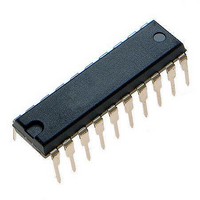
ATTINY461-20PU Atmel, ATTINY461-20PU Datasheet - Page 167

ATTINY461-20PU
Manufacturer Part Number
ATTINY461-20PU
Description
Microcontrollers (MCU) 4kB Flash 0.256kB EEPROM 16 I/O Pins
Manufacturer
Atmel
Specifications of ATTINY461-20PU
Processor Series
ATTINY4x
Core
AVR8
Data Bus Width
8 bit
Data Ram Size
256 B
Interface Type
2-Wire/SPI/USI
Maximum Clock Frequency
20 MHz
Number Of Programmable I/os
16
Number Of Timers
2
Operating Supply Voltage
4.5 V to 5.5 V
Maximum Operating Temperature
+ 85 C
Mounting Style
Through Hole
3rd Party Development Tools
EWAVR, EWAVR-BL
Development Tools By Supplier
ATAVRDRAGON, ATSTK500, ATSTK600, ATAVRISP2, ATAVRONEKIT
Minimum Operating Temperature
- 40 C
On-chip Adc
11-ch x 10-bit
Program Memory Type
Flash
Program Memory Size
4 KB
Package / Case
PDIP-20
Package
20PDIP
Device Core
AVR
Family Name
ATtiny
Maximum Speed
20 MHz
Ram Size
256 Byte
Operating Temperature
-40 to 85 °C
Lead Free Status / RoHS Status
Lead free / RoHS Compliant
- Current page: 167 of 242
- Download datasheet (5Mb)
17.5
17.6
17.6.1
17.6.2
2588E–AVR–08/10
EEPROM Write Prevents Writing to SPMCSR
Reading Fuse and Lock Bits from Software
Reading Lock Bits from Firmware
Reading Fuse Bits from Firmware
Note that an EEPROM write operation will block all software programming to Flash. Reading the
Fuses and Lock bits from software will also be prevented during the EEPROM write operation. It
is recommended that the user checks the status bit (EEPE) in the EECR Register and verifies
that the bit is cleared before writing to the SPMCSR Register.
It is possible for firmware to read device fuse and lock bits.
Note:
Lock bit values are returned in the destination register after an LPM instruction has been issued
within three CPU cycles after RFLB and SELFPRGEN bits have been set in SPMCSR. The
RFLB and SELFPRGEN bits automatically clear upon completion of reading the lock bits, or if no
LPM instruction is executed within three CPU cycles, or if no SPM instruction is executed within
four CPU cycles. When RFLB and SELFPRGEN are cleared LPM functions normally.
To read the lock bits, follow the below procedure:
If successful, the contents of the destination register are as follows.
See section
The algorithm for reading fuse bytes is similar to the one described above for reading lock bits,
only the addresses are different. To read the Fuse Low Byte (FLB), follow the below procedure:
If successful, the contents of the destination register are as follows.
Refer to
Bit
Rd
Bit
Rd
1. Load the Z-pointer with 0x0001.
2. Set RFLB and SELFPRGEN bits in SPMCSR.
3. Issue an LPM instruction within three clock cycles.
4. Read the lock bits from the LPM destination register.
1. Load the Z-pointer with 0x0000.
2. Set RFLB and SELFPRGEN bits in SPMCSR.
3. Issue an LPM instruction within three clock cycles.
4. Read the FLB from the LPM destination register.
Fuse and Lock bits that are programmed, will be read as zero. Fuse and Lock bits that are unpro-
grammed, will be read as one.
Table 18-5 on page 172
“Program And Data Memory Lock Bits” on page 170
FLB7
7
–
7
FLB6
6
–
6
for a detailed description and mapping of the Fuse Low Byte.
FLB5
5
–
5
FLB4
4
–
4
FLB3
3
–
3
FLB2
2
–
2
for more information.
FLB1
LB2
1
1
FLB0
LB1
0
0
167
Related parts for ATTINY461-20PU
Image
Part Number
Description
Manufacturer
Datasheet
Request
R

Part Number:
Description:
Manufacturer:
Atmel Corporation
Datasheet:

Part Number:
Description:
Manufacturer:
Atmel Corporation
Datasheet:

Part Number:
Description:
IC AVR MCU 4K 20MHZ 32-QFN
Manufacturer:
Atmel
Datasheet:

Part Number:
Description:
IC MCU AVR 4K FLASH 20MHZ 20SOIC
Manufacturer:
Atmel
Datasheet:

Part Number:
Description:
MCU AVR 4K FLASH 15MHZ 32-QFN
Manufacturer:
Atmel
Datasheet:

Part Number:
Description:
MCU AVR 4KB FLASH 15MHZ 32-VQFN
Manufacturer:
Atmel
Datasheet:

Part Number:
Description:
MCU AVR 4KB FLASH 20MHZ 20SOIC
Manufacturer:
Atmel
Datasheet:

Part Number:
Description:
IC MCU AVR 4K 20MHZ 32QFN
Manufacturer:
Atmel
Datasheet:

Part Number:
Description:
IC, MCU, 8BIT, 2K FLASH, 20SOIC
Manufacturer:
Atmel
Datasheet:

Part Number:
Description:
IC, MCU, 8BIT, 2K FLASH, 20PDIP
Manufacturer:
Atmel
Datasheet:


