ATTINY461-20PU Atmel, ATTINY461-20PU Datasheet - Page 119
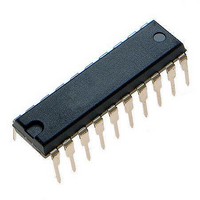
ATTINY461-20PU
Manufacturer Part Number
ATTINY461-20PU
Description
Microcontrollers (MCU) 4kB Flash 0.256kB EEPROM 16 I/O Pins
Manufacturer
Atmel
Specifications of ATTINY461-20PU
Processor Series
ATTINY4x
Core
AVR8
Data Bus Width
8 bit
Data Ram Size
256 B
Interface Type
2-Wire/SPI/USI
Maximum Clock Frequency
20 MHz
Number Of Programmable I/os
16
Number Of Timers
2
Operating Supply Voltage
4.5 V to 5.5 V
Maximum Operating Temperature
+ 85 C
Mounting Style
Through Hole
3rd Party Development Tools
EWAVR, EWAVR-BL
Development Tools By Supplier
ATAVRDRAGON, ATSTK500, ATSTK600, ATAVRISP2, ATAVRONEKIT
Minimum Operating Temperature
- 40 C
On-chip Adc
11-ch x 10-bit
Program Memory Type
Flash
Program Memory Size
4 KB
Package / Case
PDIP-20
Package
20PDIP
Device Core
AVR
Family Name
ATtiny
Maximum Speed
20 MHz
Ram Size
256 Byte
Operating Temperature
-40 to 85 °C
Lead Free Status / RoHS Status
Lead free / RoHS Compliant


12.12.5
2588E–AVR–08/10
TCCR1E – Timer/Counter1 Control Register E
• Bit 3 – FPAC1: Fault Protection Analog Comparator Enable
When written logic one, this bit enables the Fault Protection function in Timer/Counter1 to be
triggered by the Analog Comparator. The comparator output is in this case directly connected to
the Fault Protection front-end logic, making the comparator utilize the noise canceler and edge
select features of the Timer/Counter1 Fault Protection interrupt. When written logic zero, no con-
nection between the Analog Comparator and the Fault Protection function exists. To make the
comparator trigger the Timer/Counter1 Fault Protection interrupt, the FPIE1 bit in the
Timer/Counter1 Control Register D (TCCR1D) must be set.
• Bit 2 – FPF1: Fault Protection Interrupt Flag
When the FPIE1 bit is set (one), the Fault Protection Interrupt is enabled. Activity on the pin will
cause an interrupt request even, if the Fault Protection pin is configured as an output. The corre-
sponding interrupt of Fault Protection Interrupt Request is executed from the Fault Protection
Interrupt Vector. The bit FPF1 is cleared by hardware when executing the corresponding inter-
rupt handling vector. Alternatively, FPF1 is cleared after a synchronization clock cycle by writing
a logical one to the flag. When the SREG I-bit, FPIE1 and FPF1 are set, the Fault Interrupt is
executed.
• Bits 1:0 – WGM11, WGM10: Waveform Generation Mode Bits
These bits together with the PWM1A/PWM1B bits control the counting sequence of the counter
and the type of waveform generation to be used, as shown in
supported by the Timer/Counter1 are: Normal mode (counter), Fast PWM Mode, Phase and Fre-
quency Correct PWM and PWM6 Modes.
Table 12-21. Waveform Generation Mode Bit Description
• Bits 7:6 – Res: Reserved Bits
These bits are reserved and always read zero.
• Bits 5:0 – OC1OE5:OC1OE0: Output Compare Override Enable Bits
These bits are the Ouput Compare Override Enable bits that are used to connect or disconnect
the Output Compare Pins in PWM6 Modes with an instant response on the corresponding Out-
put Compare Pins. The actual value from the port register will be visible on the port pin, when
Bit
0x00 (0x20)
Read/Write
Initial value
PWM1A/
PWM1B
0
1
1
1
1
WGM11:10
R
7
0
-
XX
00
01
10
11
R
6
0
-
Timer/Counter
Mode of Operation
Normal
Fast PWM
Phase & Frequency Correct PWM
PWM6 / Single-slope
PWM6 / Dual-slope
OC1OE5
R/W
5
0
OC1OE4
R/W
4
0
OC1OE3
R/W
3
0
OC1OE2
TOP
OCR1C
OCR1C
OCR1C
OCR1C
OCR1C
R/W
Table
2
0
12-21. Modes of operation
OC1OE1
R/W
1
0
Update
OCR1x at
Immediate
TOP
BOTTOM
TOP
BOTTOM
OC1OE0
R/W
0
0
Set TOV1
Flag at
TOP
TOP
BOTTOM
TOP
BOTTOM
TCCR1E
119
Related parts for ATTINY461-20PU
Image
Part Number
Description
Manufacturer
Datasheet
Request
R

Part Number:
Description:
Manufacturer:
Atmel Corporation
Datasheet:
Part Number:
Description:
Manufacturer:
Atmel Corporation
Datasheet:

Part Number:
Description:
IC AVR MCU 4K 20MHZ 32-QFN
Manufacturer:
Atmel
Datasheet:

Part Number:
Description:
IC MCU AVR 4K FLASH 20MHZ 20SOIC
Manufacturer:
Atmel
Datasheet:

Part Number:
Description:
MCU AVR 4K FLASH 15MHZ 32-QFN
Manufacturer:
Atmel
Datasheet:
Part Number:
Description:
MCU AVR 4KB FLASH 15MHZ 32-VQFN
Manufacturer:
Atmel
Datasheet:
Part Number:
Description:
MCU AVR 4KB FLASH 20MHZ 20SOIC
Manufacturer:
Atmel
Datasheet:


Part Number:
Description:
IC MCU AVR 4K 20MHZ 32QFN
Manufacturer:
Atmel
Datasheet:
Part Number:
Description:
IC, MCU, 8BIT, 2K FLASH, 20SOIC
Manufacturer:
Atmel
Datasheet:

Part Number:
Description:
IC, MCU, 8BIT, 2K FLASH, 20PDIP
Manufacturer:
Atmel
Datasheet: