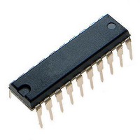
ATTINY461-20PU Atmel, ATTINY461-20PU Datasheet - Page 131

ATTINY461-20PU
Manufacturer Part Number
ATTINY461-20PU
Description
Microcontrollers (MCU) 4kB Flash 0.256kB EEPROM 16 I/O Pins
Manufacturer
Atmel
Specifications of ATTINY461-20PU
Processor Series
ATTINY4x
Core
AVR8
Data Bus Width
8 bit
Data Ram Size
256 B
Interface Type
2-Wire/SPI/USI
Maximum Clock Frequency
20 MHz
Number Of Programmable I/os
16
Number Of Timers
2
Operating Supply Voltage
4.5 V to 5.5 V
Maximum Operating Temperature
+ 85 C
Mounting Style
Through Hole
3rd Party Development Tools
EWAVR, EWAVR-BL
Development Tools By Supplier
ATAVRDRAGON, ATSTK500, ATSTK600, ATAVRISP2, ATAVRONEKIT
Minimum Operating Temperature
- 40 C
On-chip Adc
11-ch x 10-bit
Program Memory Type
Flash
Program Memory Size
4 KB
Package / Case
PDIP-20
Package
20PDIP
Device Core
AVR
Family Name
ATtiny
Maximum Speed
20 MHz
Ram Size
256 Byte
Operating Temperature
-40 to 85 °C
Lead Free Status / RoHS Status
Lead free / RoHS Compliant
- Current page: 131 of 242
- Download datasheet (5Mb)
13.3.5
13.3.6
2588E–AVR–08/10
Start Condition Detector
Clock speed considerations
If the slave is not able to receive more data it does not acknowledge the data byte it has last
received. When the master does a read operation it must terminate the operation by forcing the
acknowledge bit low after the last byte transmitted.
The start condition detector is shown in
to 300 ns) to ensure valid sampling of the SCL line. The start condition detector is only enabled
in Two-wire mode.
Figure 13-6. Start Condition Detector, Logic Diagram
The start condition detector works asynchronously and can therefore wake up the processor
from power-down sleep mode. However, the protocol used might have restrictions on the SCL
hold time. Therefore, when using this feature in this case the Oscillator start-up time set by the
CKSEL Fuses (see
to the USISIF bit description on page 133 for further details.
Maximum frequency for SCL and SCK is f
receive rate in both two- and three-wire mode. In two-wire slave mode the Two-wire Clock Con-
trol Unit will hold the SCL low until the slave is ready to receive more data. This may reduce the
actual data rate in two-wire mode.
3. The master set the first bit to be transferred and releases the SCL line (C). The slave
4. After eight bits containing slave address and data direction (read or write) have been
5. When the slave is addressed, it holds the SDA line low during the acknowledgment
6. Multiple bytes can now be transmitted, all in same direction, until a stop condition is
samples the data and shifts it into the USI Data Register at the positive edge of the SCL
clock.
transferred, the slave counter overflows and the SCL line is forced low (D). If the slave
is not the one the master has addressed, it releases the SCL line and waits for a new
start condition.
cycle before holding the SCL line low again (i.e., the USI Counter Register must be set
to 14 before releasing SCL at (D)). Depending on the R/W bit the master or slave
enables its output. If the bit is set, a master read operation is in progress (i.e., the slave
drives the SDA line) The slave can hold the SCL line low after the acknowledge (E).
given by the master (F), or a new start condition is given.
Write( USISIF)
“Clock System” on page
SDA
SCL
Figure
CK
24) must also be taken into the consideration. Refer
/ 2. This is also the maximum data transmit and
13-6. The SDA line is delayed (in the range of 50
D Q
CLR
D Q
CLR
USISIF
CLOCK
HOLD
131
Related parts for ATTINY461-20PU
Image
Part Number
Description
Manufacturer
Datasheet
Request
R

Part Number:
Description:
Manufacturer:
Atmel Corporation
Datasheet:

Part Number:
Description:
Manufacturer:
Atmel Corporation
Datasheet:

Part Number:
Description:
IC AVR MCU 4K 20MHZ 32-QFN
Manufacturer:
Atmel
Datasheet:

Part Number:
Description:
IC MCU AVR 4K FLASH 20MHZ 20SOIC
Manufacturer:
Atmel
Datasheet:

Part Number:
Description:
MCU AVR 4K FLASH 15MHZ 32-QFN
Manufacturer:
Atmel
Datasheet:

Part Number:
Description:
MCU AVR 4KB FLASH 15MHZ 32-VQFN
Manufacturer:
Atmel
Datasheet:

Part Number:
Description:
MCU AVR 4KB FLASH 20MHZ 20SOIC
Manufacturer:
Atmel
Datasheet:

Part Number:
Description:
IC MCU AVR 4K 20MHZ 32QFN
Manufacturer:
Atmel
Datasheet:

Part Number:
Description:
IC, MCU, 8BIT, 2K FLASH, 20SOIC
Manufacturer:
Atmel
Datasheet:

Part Number:
Description:
IC, MCU, 8BIT, 2K FLASH, 20PDIP
Manufacturer:
Atmel
Datasheet:


