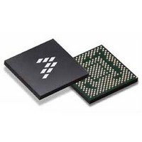
SC900841JVK Freescale Semiconductor, SC900841JVK Datasheet - Page 123

SC900841JVK
Manufacturer Part Number
SC900841JVK
Description
IC POWER MGT 338-MAPBGA
Manufacturer
Freescale Semiconductor
Specifications of SC900841JVK
Applications
PC's, PDA's
Operating Temperature
-40°C ~ 85°C
Mounting Type
Surface Mount
Package / Case
338-TBGA
Input Voltage
2.8 V to 4.4 V
Maximum Operating Temperature
+ 85 C
Minimum Operating Temperature
- 40 C
Lead Free Status / RoHS Status
Lead free / RoHS Compliant
Current - Supply
-
Voltage - Supply
-
Lead Free Status / Rohs Status
Lead free / RoHS Compliant
Available stocks
Company
Part Number
Manufacturer
Quantity
Price
Company:
Part Number:
SC900841JVK
Manufacturer:
Freescale Semiconductor
Quantity:
10 000
Company:
Part Number:
SC900841JVKR2
Manufacturer:
Freescale Semiconductor
Quantity:
10 000
- Current page: 123 of 192
- Download datasheet (8Mb)
VPWR node where all on-chip regulators draw their power
from at a typical operating range of 3.0 to 4.4 V. See
Figure
pin, the respective input voltage is converted to a variable
output voltage at the VPWR node through a buck switching
DC/DC regulator, Charger buck.
CHARGER BUCK OPERATION
depending on the state of the battery:
Analog Integrated Circuit Device Data
Freescale Semiconductor
The multiplexed power output is made available at the
Charger buck takes its feedback from two sources,
• For batteries with a voltage less than the trickle charge
threshold, V
supply the system loads. The feedback is taken from a
conventional internal resistor divider connected at the
VPWR pin. This supports dead battery operation and
62. When a power source is detected at the RAWCHG
Interface
Local
Bus
SPI
+
CHRENB
BATISO
TEMP
TEMPEN
COMP
BATOCPSET
CHRGTIMER
CHRGCC
CHRGCV
TRICKLE
WDTSET
BATDET
CHGBYP
USBOVP
USBLMT
RDSTATE
CHRGCOMP
RDSTEN
OVRVOLT
BATOVP
USBDET
CHR
OTGB
WDTEN
DCLMT
ITRKL
PWR
is set at a constant voltage of 4.2 V to
Multiplexed Feedback+
Reference
Figure 62. Power Path Manager + Li-Ion Charger Block Diagram
PWM
Buck
Charger Control +
Timer
Level Detection
Input Voltage
Dead-
Driver
Gate
time
+
Control
Battery
Switch
LDO
V
NTC Interface
CORE
Moniroting
Coulomb
Counter
Current
Voltage
Monitor
Battery
Battery
Charge
Trickle
Moniroting
Current
Input
modes. The charger buck needs to be able to support 100%
duty operation for cases when the input falls close to the
output voltage. In this mode, M
and M
close to it) duty-cycle mode until either V
4.7V, under which case V
4.7V, or the loop feedback demands a lower duty cycle. While
• For batteries within normal operation of 3.0 to 4.4 V,
The buck regulator core implements PWM and auto-PFM
BATTERY INTERFACE AND POWER PATH MANAGEMENT
allows the system to operate if the battery does not
exist, or is being trickle charged through a separate
path.
V
power dissipation low during charging, VPWR is
normally adjusted to be 300 mV above V
a maximum of 4.7 V.
LSCHG
PWR
CHGBYPGT
RAWCHG
CHGGT
ISNSBATP
ISNSBATN
VBAT
OVPCHGGT
REVPCHGGT
PVINCHG
VPWR
CFM
GNDBAT
ISNSINN
HSCHGGT
SWFBCHG
CFP
VNTC
ISNSINP
LSCHGGT
PGNDCHG
NTC
tracks the battery voltage level V
is disabled. The regulator will stay in 100% (or
USB OR AC
C
CC
R
INSNSCHG
M
M
M
M
REVPCHG
HSCHG
OVPCHG
LSCHG
PWR
FUNCTIONAL DEVICE OPERATION
L
CHG
Optional:
20V maximum surge
protection
is clamped to a maximum of
HSCHG
R
C
R
M
SNSBAT
C
INCHG
CC
CHG
RAWCHG
From VOTG
C
is switched fully on,
V
OCHG
PWR
NTC
PWR
System Loads
R
Optional:
Reduce Series Drop
when Discharging
BAT
NTC
rises above
BAT
M
CHGBYP
. To keep
, subject to
900841
123
Related parts for SC900841JVK
Image
Part Number
Description
Manufacturer
Datasheet
Request
R
Part Number:
Description:
Manufacturer:
Freescale Semiconductor, Inc
Datasheet:
Part Number:
Description:
Manufacturer:
Freescale Semiconductor, Inc
Datasheet:
Part Number:
Description:
Manufacturer:
Freescale Semiconductor, Inc
Datasheet:
Part Number:
Description:
Manufacturer:
Freescale Semiconductor, Inc
Datasheet:
Part Number:
Description:
Manufacturer:
Freescale Semiconductor, Inc
Datasheet:
Part Number:
Description:
Manufacturer:
Freescale Semiconductor, Inc
Datasheet:
Part Number:
Description:
Manufacturer:
Freescale Semiconductor, Inc
Datasheet:
Part Number:
Description:
Manufacturer:
Freescale Semiconductor, Inc
Datasheet:
Part Number:
Description:
Manufacturer:
Freescale Semiconductor, Inc
Datasheet:
Part Number:
Description:
Manufacturer:
Freescale Semiconductor, Inc
Datasheet:
Part Number:
Description:
Manufacturer:
Freescale Semiconductor, Inc
Datasheet:
Part Number:
Description:
Manufacturer:
Freescale Semiconductor, Inc
Datasheet:
Part Number:
Description:
Manufacturer:
Freescale Semiconductor, Inc
Datasheet:
Part Number:
Description:
Manufacturer:
Freescale Semiconductor, Inc
Datasheet:
Part Number:
Description:
Manufacturer:
Freescale Semiconductor, Inc
Datasheet:


