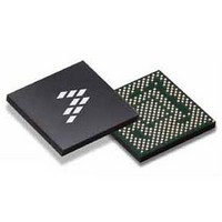
SC900841JVK Freescale Semiconductor, SC900841JVK Datasheet - Page 47

SC900841JVK
Manufacturer Part Number
SC900841JVK
Description
IC POWER MGT 338-MAPBGA
Manufacturer
Freescale Semiconductor
Specifications of SC900841JVK
Applications
PC's, PDA's
Operating Temperature
-40°C ~ 85°C
Mounting Type
Surface Mount
Package / Case
338-TBGA
Input Voltage
2.8 V to 4.4 V
Maximum Operating Temperature
+ 85 C
Minimum Operating Temperature
- 40 C
Lead Free Status / RoHS Status
Lead free / RoHS Compliant
Current - Supply
-
Voltage - Supply
-
Lead Free Status / Rohs Status
Lead free / RoHS Compliant
Available stocks
Company
Part Number
Manufacturer
Quantity
Price
Company:
Part Number:
SC900841JVK
Manufacturer:
Freescale Semiconductor
Quantity:
10 000
Company:
Part Number:
SC900841JVKR2
Manufacturer:
Freescale Semiconductor
Quantity:
10 000
- Current page: 47 of 192
- Download datasheet (8Mb)
PWRGD Pin
Platform controller hub. Assertion of PWRGD means that the
VCCPAOAC, VAON, and VPMIC rails have been valid for at
least 100 microseconds. The Platform Controller Hub will
remain off until this signal is asserted. This signal is only de-
asserted if VCCPAOAC, VAON, or VPMIC is out of
regulation, or a cold reset is initiated by the firmware.
Table 3
WARM and COLD RESET
which are initiated through the register file. Together they
define a warm reset or cold reset to the Platform controller
hub. The sequencing shown in
from the register CHIPCNTRL through bits WARMRST and
COLDRST. The pulse should be held low for 5s < t < 31s.|
Analog Integrated Circuit Device Data
Freescale Semiconductor
This is a Power Good Output Signal from the 900841 to the
The PWRGD pin follows the DC Signaling specifications in
The RESET and PWRGD signals have two functions
with a reference of 1.8 V (VPMIC)
Figure 10. Warm/Cold Reset Functionality
Figure 10
and is controlled
Table 13. CHIPCNTL Register Structure and Bit
EXITSTBY Pin
exits the AOAC standby settings for regulating the platform
supplies. When asserted, the PMIC switches the voltage
regulators, as defined in the voltage regulator registers from
the CTL Bits to the AOACTL Bits. This is a low latency voltage
regulators context switch.
Table 3
AOAC Exit Standby
Platform controller hub, the VRCOMP signal should be driven
low. On the rising edge of the EXITSTBY signal, the AOACTL
bits should be copied to the CTL bits in the different voltage
regulator control registers, unless Bit 5 is '0'. If Bit 5 is '0', then
the CTL bits are not modified. The VRCOMP signal is de-
asserted at this point. Next the rails defined in the new CTL
registers should be ramped up together or remain in the
same state, as if the AOACTL settings were the same as the
previous CTL setting. Once all of the rails are in regulation,
the VRCOMP signal should be driven high.
signal. There is a special case (Optimized Case) when the
EXITSTBY signal is asserted with the VCCP, VCCPDDR,
VCCA, and VCC180 rails. If some combination of these four
rails turn on with the assertion of the EXITSTBY signal, the
entire time for the re-configuration should take no longer than
30 ms. See
WARMRST
COLDRST
When the EXITSTBY pin is asserted high, the 900841
EXITSTBY pin follows the DC signaling specifications in
When the EXITSTBY signal is asserted high from the
Figure 11
Reserved
Name
CHIPCNTL (ADDR 0x 06 - R/W - Default Value: 0x00)
with a reference of 1.05 V (VCCP)
Description
Figure
shows the timing diagram of the EXITSTBY
Bits
7:2
0
1
12.
Cold Reset Function Enable
x0 = No Change
x1 = Pulse RESET and PWRGD Low
Warm Reset Function Enable
x0 = No Change
x1 = Pulse RESET Low
Reserved
FUNCTIONAL DEVICE OPERATION
SYSTEM CONTROL INTERFACE
Description
900841
47
Related parts for SC900841JVK
Image
Part Number
Description
Manufacturer
Datasheet
Request
R
Part Number:
Description:
Manufacturer:
Freescale Semiconductor, Inc
Datasheet:
Part Number:
Description:
Manufacturer:
Freescale Semiconductor, Inc
Datasheet:
Part Number:
Description:
Manufacturer:
Freescale Semiconductor, Inc
Datasheet:
Part Number:
Description:
Manufacturer:
Freescale Semiconductor, Inc
Datasheet:
Part Number:
Description:
Manufacturer:
Freescale Semiconductor, Inc
Datasheet:
Part Number:
Description:
Manufacturer:
Freescale Semiconductor, Inc
Datasheet:
Part Number:
Description:
Manufacturer:
Freescale Semiconductor, Inc
Datasheet:
Part Number:
Description:
Manufacturer:
Freescale Semiconductor, Inc
Datasheet:
Part Number:
Description:
Manufacturer:
Freescale Semiconductor, Inc
Datasheet:
Part Number:
Description:
Manufacturer:
Freescale Semiconductor, Inc
Datasheet:
Part Number:
Description:
Manufacturer:
Freescale Semiconductor, Inc
Datasheet:
Part Number:
Description:
Manufacturer:
Freescale Semiconductor, Inc
Datasheet:
Part Number:
Description:
Manufacturer:
Freescale Semiconductor, Inc
Datasheet:
Part Number:
Description:
Manufacturer:
Freescale Semiconductor, Inc
Datasheet:
Part Number:
Description:
Manufacturer:
Freescale Semiconductor, Inc
Datasheet:


