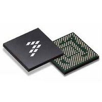
SC900841JVK Freescale Semiconductor, SC900841JVK Datasheet - Page 173

SC900841JVK
Manufacturer Part Number
SC900841JVK
Description
IC POWER MGT 338-MAPBGA
Manufacturer
Freescale Semiconductor
Specifications of SC900841JVK
Applications
PC's, PDA's
Operating Temperature
-40°C ~ 85°C
Mounting Type
Surface Mount
Package / Case
338-TBGA
Input Voltage
2.8 V to 4.4 V
Maximum Operating Temperature
+ 85 C
Minimum Operating Temperature
- 40 C
Lead Free Status / RoHS Status
Lead free / RoHS Compliant
Current - Supply
-
Voltage - Supply
-
Lead Free Status / Rohs Status
Lead free / RoHS Compliant
Available stocks
Company
Part Number
Manufacturer
Quantity
Price
Company:
Part Number:
SC900841JVK
Manufacturer:
Freescale Semiconductor
Quantity:
10 000
Company:
Part Number:
SC900841JVKR2
Manufacturer:
Freescale Semiconductor
Quantity:
10 000
- Current page: 173 of 192
- Download datasheet (8Mb)
Table 115. GPO Register Structure and Bits Description
Table 114. GPIO/GPOSW Register Structure and Bits Description
Analog Integrated Circuit Device Data
Freescale Semiconductor
Notes
SCRATCHx 6:7
SWDOUTx
SWDRVx
34.
35.
GPIINT4
GPIINT5
GPIINT6
GPIINT7
GPO0
GPO1
Name
SLEWx
Name
-
-
See GPIOs electrical characteristics on
An unintended interrupt is caused if interrupt settings are reconfigured in the middle of an application, e.g. re-setting interrupt detection
from detecting an interrupt on both edges to an interrupt on the rising edge. To mask any unwanted interrupt, change the GPIO interrupt
detection to the new configuration, then clear Level 1 and level 2 interrupts. Finally unmask the GPIO Interrupt.
Bits
Bits
4:5
0
1
4
5
6
7
0
1
2
3
GPIO4 Interrupt Flag
x0 = No Interrupt occurred or Masked Interrupt
x1 = Interrupt occurred
GPIO5 Interrupt Flag
x0 = No Interrupt occurred or Masked Interrupt
x1 = Interrupt occurred
GPIO6 Interrupt Flag
x0 = No Interrupt occurred or Masked Interrupt
x1 = Interrupt occurred
GPIO7 Interrupt Flag
x0 = No Interrupt occurred or Masked Interrupt
x1 = Interrupt occurred
GPOSWx Output Driver Type
x0 = Open Drain
x1 = CMOS
RESERVED
RESERVED
The value in the SWDOUTx bit reflects the desired electrical output state of the GPOSWx pin.
X0 = Electrical Low
x1 = Electrical High (CMOS) or High-impedance Output (Open-drain)
The value of the SLEWx Bits determines the level of slew rate control being exercised on the output’s ramp rates. The level
of slew rate control exercised is expected to hold true for both CMOS and Open Drain outputs. However, in the case of
Open Drain outputs, the specified ramp rate is assuming an externally connected 100 k
parallel capacitance).
These values are met at the lowest supply voltage, GPOSWVCC = 1.8 V
X0 = 50
X1 = 2.0 k
X2 = 20 k
X3 = 200 k
These bits shall not exert any control over the operation of the GPOSWx, and are intended to be used as scratchpad
registers by the system controller. Their contents are erased on POR.
GPO0 Output Level
x0 = Low0
x1 = High (To voltage supplied on GPOVCC Pin)
GPO1 Output Level
x0 = Low
x1 = High (To voltage supplied on GPOVCC Pin)
Ω
Ω
Ω
Ω
max (NFET) – 100
, ±35% at room temperature
, ±35% at room temperature
, ±25% at room temperature
(34)
GPO (ADDR 0xF4 - R/W - Default Value: 0x00)
Table 3
Ω
max (PFET)
GPOSWCTLx (x = 0 to 3)
Description
Description
(34)
FUNCTIONAL DEVICE OPERATION
Ω
(±1%) pull-up resistor (and no
GPIOS
900841
173
Related parts for SC900841JVK
Image
Part Number
Description
Manufacturer
Datasheet
Request
R
Part Number:
Description:
Manufacturer:
Freescale Semiconductor, Inc
Datasheet:
Part Number:
Description:
Manufacturer:
Freescale Semiconductor, Inc
Datasheet:
Part Number:
Description:
Manufacturer:
Freescale Semiconductor, Inc
Datasheet:
Part Number:
Description:
Manufacturer:
Freescale Semiconductor, Inc
Datasheet:
Part Number:
Description:
Manufacturer:
Freescale Semiconductor, Inc
Datasheet:
Part Number:
Description:
Manufacturer:
Freescale Semiconductor, Inc
Datasheet:
Part Number:
Description:
Manufacturer:
Freescale Semiconductor, Inc
Datasheet:
Part Number:
Description:
Manufacturer:
Freescale Semiconductor, Inc
Datasheet:
Part Number:
Description:
Manufacturer:
Freescale Semiconductor, Inc
Datasheet:
Part Number:
Description:
Manufacturer:
Freescale Semiconductor, Inc
Datasheet:
Part Number:
Description:
Manufacturer:
Freescale Semiconductor, Inc
Datasheet:
Part Number:
Description:
Manufacturer:
Freescale Semiconductor, Inc
Datasheet:
Part Number:
Description:
Manufacturer:
Freescale Semiconductor, Inc
Datasheet:
Part Number:
Description:
Manufacturer:
Freescale Semiconductor, Inc
Datasheet:
Part Number:
Description:
Manufacturer:
Freescale Semiconductor, Inc
Datasheet:


