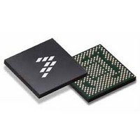
SC900841JVK Freescale Semiconductor, SC900841JVK Datasheet - Page 53

SC900841JVK
Manufacturer Part Number
SC900841JVK
Description
IC POWER MGT 338-MAPBGA
Manufacturer
Freescale Semiconductor
Specifications of SC900841JVK
Applications
PC's, PDA's
Operating Temperature
-40°C ~ 85°C
Mounting Type
Surface Mount
Package / Case
338-TBGA
Input Voltage
2.8 V to 4.4 V
Maximum Operating Temperature
+ 85 C
Minimum Operating Temperature
- 40 C
Lead Free Status / RoHS Status
Lead free / RoHS Compliant
Current - Supply
-
Voltage - Supply
-
Lead Free Status / Rohs Status
Lead free / RoHS Compliant
Available stocks
Company
Part Number
Manufacturer
Quantity
Price
Company:
Part Number:
SC900841JVK
Manufacturer:
Freescale Semiconductor
Quantity:
10 000
Company:
Part Number:
SC900841JVKR2
Manufacturer:
Freescale Semiconductor
Quantity:
10 000
Table 22. PLL Control Register Structure and Bit
CLOCK GENERATION
well as for external applications utilizing the clock output pins.
A crystal oscillator is used for the 32.768 kHz time base and
generation of related derivative clocks. If the crystal oscillator
is not running (for example, if the crystal is not present), an
internal 32 kHz oscillator will be used instead.
26 MHz clock for Audio usage. This clock is also routed to the
companion chip, 900842, through the CLK26M pin.
Clocking Scheme
the crystal oscillator and provides a 32.768 kHz nominal
frequency at 50% accuracy, if running. The internal oscillator
only runs if a valid supply is available at the charger input,
battery, or coin cell, and would not be used as long as the
crystal oscillator is active. The crystal oscillator continues
running, supplied from one of the sources as described
previously, until all power is depleted or removed. All control
functions will run off the crystal derived frequency,
occasionally referred to as the "32 kHz".
CLK32K output pin, which is SPIVCC referenced. CLK32K is
provided as a peripheral clock reference. The driver is
enabled by the startup sequencer. Additionally, a SPI bit
PLLDIVIDE
PLL16MEN
Analog Integrated Circuit Device Data
Freescale Semiconductor
Reserved
PLLEN
Name
A system clock is generated for internal digital circuitry, as
In addition, another crystal oscillator is used to generate a
The internal 32 kHz oscillator is an integrated backup for
At system startup, the 32 kHz clock is driven to the
FSLPLLCNTL (ADDR 0x1E4 - R/W - Default Value: 0x1B)
Description
Bits
2:0
7:5
3
4
PLL Divide Ratio and Effective VCO
Frequency Settings
x0 = 112, 3.670 MHz
x1 = 116, 3.801 MHz
x2 = 120, 3.932 MHz
x3 = 124, 4.063 MHz
x4 = 128, 4.194 MHz
x5 = 132, 4.325 MHz
x6 = 136, 4.456 MHz
x7 = 140, 4.588 MHz
16 MHz frequency enable
x0 = 16 MHz clock disabled
x1 = 16 MHz clock enabled and PLL enabled
PLL Enable, even if there is no block
requesting a clock
x0 = PLL enabled based on device enables
only
x1 = PLL enabled
Reserved
CLOCK GENERATION AND REAL TIME CLOCK (RTC)
Description
TEST MODES
Test Mode Configuration
normal operation or test mode via the ICTEST pin and other
register configurations. Details of Test mode programmability
are not documented herein, but should be referenced from
other Design for Test documentation.
accessed in applications. In test modes, signals are
multiplexed on existing functional pins. The ICTEST pin must
therefore be tied to ground (for normal operation) at the board
level, in product applications
temperature op life testing. A proprietary protocol is included
for scan chain test configurations, which reuses the SPI pins.
In-package Trimming
package, such as the main bandgap, and other precision
analog functions. Trim registers are for Freescale use only
and must not be accessed in product applications. Fuse
programming circuitry will be blocked during normal and test
mode operation.
M32KCLK bit is provided for direct SPI control. The
M32KCLK bit defaults to 0 to enable the driver and resets on
the RTCPORB to ensure the buffer is activated at the first
power up and configured as desired, for subsequent power
ups.
with CLK32KDRV[1:0] (master control bits that affect the
drive strength of CLK32K), see FSLOUTDRVCNTL2
Register in
(such as when the crystal oscillator is starting up), it will occur
during the active low phase of both clocks, to avoid clocking
glitches. A status bit, OSCSTP, is available to indicate to the
processor which clock is currently selected: OSCSTP=1
when the internal RC is used, and OSCSTP=0 if the XTAL
source is used.
operation for the Audio block of 900841. The 26 MHz signal
is needed internally for Audio operation, but is also provided
to the companion chip, 900842, via the CLK26M output pin
when the V33 voltage rail is enabled..
with CLK26MDRV[1:0] (master control bits that affect the
drive strength of CLK26M), see the FSLOUTDRVCNTL2
Register in
During evaluation and testing, the IC can be configured for
Test modes are for Freescale use only, and must not be
Test mode also disables the thermal protection for high
During IC final test, several parameters are trimmed in the
The drive strength of the output drivers is programmable
If a switchover occurs between the two clock sources
The 26 MHz XTAL is necessary to provide a low jitter clock
The drive strength of the output drivers is programmable
CLOCK GENERATION AND REAL TIME CLOCK (RTC)
Table
Table
21.
21.
FUNCTIONAL DEVICE OPERATION
900841
53


