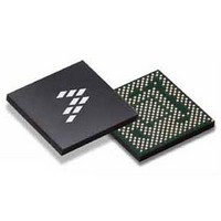
SC900841JVK Freescale Semiconductor, SC900841JVK Datasheet - Page 135

SC900841JVK
Manufacturer Part Number
SC900841JVK
Description
IC POWER MGT 338-MAPBGA
Manufacturer
Freescale Semiconductor
Specifications of SC900841JVK
Applications
PC's, PDA's
Operating Temperature
-40°C ~ 85°C
Mounting Type
Surface Mount
Package / Case
338-TBGA
Input Voltage
2.8 V to 4.4 V
Maximum Operating Temperature
+ 85 C
Minimum Operating Temperature
- 40 C
Lead Free Status / RoHS Status
Lead free / RoHS Compliant
Current - Supply
-
Voltage - Supply
-
Lead Free Status / Rohs Status
Lead free / RoHS Compliant
Available stocks
Company
Part Number
Manufacturer
Quantity
Price
Company:
Part Number:
SC900841JVK
Manufacturer:
Freescale Semiconductor
Quantity:
10 000
Company:
Part Number:
SC900841JVKR2
Manufacturer:
Freescale Semiconductor
Quantity:
10 000
- Current page: 135 of 192
- Download datasheet (8Mb)
VOICE CODEC PROTOCOL
both single word per frame and multiple words per frame
time-division multiplexed (TDM) modes, and can be used in
either master or slave mode. Master mode is selected by
setting the VCEMASTEN bit. In master mode, the voice
Table 82. Interface Driver Characteristics
Table 83. Interface Timing Specifications
Analog Integrated Circuit Device Data
Freescale Semiconductor
BCL1, BCL2, FS1, FS2 Rise and Fall Time
The serial interface protocol for the voice codec supports
B C L
F S (S h o rt)
F S (L o n g )
T X
R X
Parameter
t
SYNCHOLD
t
t
t
ENDSYNC
SYNCSET
CLKSYNC
t
t
SYNCTX
t
t
HIZOUT
t
t
CLKTX
SETUP
t
CLKH
HOLD
t
CLKL
CLK
if in Master mode
T s yn c se t
Delay time from clock edge to TX for short sync
Delay time from BCL to long sync low after LSB
Delay time from long sync to TX (slave mode)
Sync setup time for short sync (master mode)
Sync hold time for short sync (master mode)
Sync setup time for short sync (slave mode)
Sync hold time for short sync (slave mode)
Delay time from LSB of TX to Hi-Z state
Delay time from clock to long sync
T sy n ch o ld
BCL clock frequency
Set-up time for RX
SSIDRV[1:0]=00 (default)
Figure 67. Interface Timing Diagram
Hold time for RX
BCL clock high
BCL clock low
Description
T clks yn c
SSIDRV[1:0]=01
SSIDRV[1:0]=10
SSIDRV[1:0]=11
T c lk tx
H i-Z
T c lkh
T s e tu p
codec generates the bit clock and frame sync signals, as long
as the VCECLKEN bit is set. The data is transmitted and
received in a two's complement format, MSB first, and can be
clocked on the positive or negative edge of the bit clock. The
active edge of the bit clock can be selected by the
VCEBCLINV bit. The interface can operate with a short (bit
T s yn c tx
M S B / L S B
M S B / L S B
T clk
T h o ld
T c lkl
Min
128
220
220
200
200
20
20
20
20
20
20
-
-
-
High Z
11
22
H i-Z
6
FUNCTIONAL DEVICE OPERATION
T e n d s yn c
T h iz o u t
Typ
-
-
-
-
-
-
-
-
-
-
-
-
-
-
2048
Max
15
20
20
-
-
-
-
-
-
-
-
-
-
Unit
kHz
AUDIO
ns
ns
ns
ns
ns
ns
ns
ns
ns
ns
ns
ns
ns
ns
ns
ns
ns
900841
135
Related parts for SC900841JVK
Image
Part Number
Description
Manufacturer
Datasheet
Request
R
Part Number:
Description:
Manufacturer:
Freescale Semiconductor, Inc
Datasheet:
Part Number:
Description:
Manufacturer:
Freescale Semiconductor, Inc
Datasheet:
Part Number:
Description:
Manufacturer:
Freescale Semiconductor, Inc
Datasheet:
Part Number:
Description:
Manufacturer:
Freescale Semiconductor, Inc
Datasheet:
Part Number:
Description:
Manufacturer:
Freescale Semiconductor, Inc
Datasheet:
Part Number:
Description:
Manufacturer:
Freescale Semiconductor, Inc
Datasheet:
Part Number:
Description:
Manufacturer:
Freescale Semiconductor, Inc
Datasheet:
Part Number:
Description:
Manufacturer:
Freescale Semiconductor, Inc
Datasheet:
Part Number:
Description:
Manufacturer:
Freescale Semiconductor, Inc
Datasheet:
Part Number:
Description:
Manufacturer:
Freescale Semiconductor, Inc
Datasheet:
Part Number:
Description:
Manufacturer:
Freescale Semiconductor, Inc
Datasheet:
Part Number:
Description:
Manufacturer:
Freescale Semiconductor, Inc
Datasheet:
Part Number:
Description:
Manufacturer:
Freescale Semiconductor, Inc
Datasheet:
Part Number:
Description:
Manufacturer:
Freescale Semiconductor, Inc
Datasheet:
Part Number:
Description:
Manufacturer:
Freescale Semiconductor, Inc
Datasheet:


