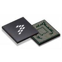
SC900841JVK Freescale Semiconductor, SC900841JVK Datasheet - Page 52

SC900841JVK
Manufacturer Part Number
SC900841JVK
Description
IC POWER MGT 338-MAPBGA
Manufacturer
Freescale Semiconductor
Specifications of SC900841JVK
Applications
PC's, PDA's
Operating Temperature
-40°C ~ 85°C
Mounting Type
Surface Mount
Package / Case
338-TBGA
Input Voltage
2.8 V to 4.4 V
Maximum Operating Temperature
+ 85 C
Minimum Operating Temperature
- 40 C
Lead Free Status / RoHS Status
Lead free / RoHS Compliant
Current - Supply
-
Voltage - Supply
-
Lead Free Status / Rohs Status
Lead free / RoHS Compliant
Available stocks
Company
Part Number
Manufacturer
Quantity
Price
Company:
Part Number:
SC900841JVK
Manufacturer:
Freescale Semiconductor
Quantity:
10 000
Company:
Part Number:
SC900841JVKR2
Manufacturer:
Freescale Semiconductor
Quantity:
10 000
- Current page: 52 of 192
- Download datasheet (8Mb)
Table 18. General Purpose Memory MEMx Register
Table 17. Vendor ID Registers Structure and Bits
SPECIAL REGISTERS
Vendor ID and Version ID
the Identification bits. These are hard-wired on the chip.
Embedded Memory
memory, accessible by the processor to store critical data
during power down. The data written to these registers is
maintained by the coin cell when the main battery is deeply
discharged or removed, and is part of the RTC block. The
content of the embedded memory is reset by RTCPORB. The
banks can be used for any system need, for bit retention with
coin cell backup.
dedicated register space.
52
900841
FUNCTIONAL DEVICE OPERATION
SYSTEM CONTROL INTERFACE
VENDID1
Reserved
VENDID2
Reserved
Reserved
Reserved
Register
The Vendor ID and other version details can be read via
There are 24 register banks of general purpose embedded
X is from 1 to 8 in
MEMx
The rest of the 24 registers reside in the Freescale
X is from 1 to 16 in the following table
Name
REV1
REV2
ID1 (ADDR 0x00 - R - Default Value: 0x28)
ID2 (ADDR 0x01 - R - Default Value: 0x00)
ID3 (ADDR 0x02 - R - Default Value: 0x00)
ID4 (ADDR 0x03 - R - Default Value: 0x00)
Structure and Bits Description
Description
Name
Bits
2:0
5:3
7:6
2:0
5:3
7:6
7:0
7:0
-
Table
Chip1 Vendor ID
Chip1 Revision ID
Reserved
Chip2 Vendor ID
Chip2 Revision ID
Reserved
Reserved
Reserved
Bits
7:0
18.
General Purpose Memory
Register x
Description
Description
Table 20. Output Driver Control Selection
Table 21. Output Driver Register Structure and Bit
Table 19. General Purpose Memory FSLMEMx Register
Output Driver Control
programmed for 4 different settings as shows in the following
tables. All of the following outputs follow the settings as
shown.
PLL Control
divider values for different output frequencies.
VRCOMPBDRV
FSLMEMx
FSLOUTDRVCNTL1 (ADDR 0x1BF - R/W - Default Value: 0x00)
FSLOUTDRVCNTL2 (ADDR 0x1C0 - R/W - Default Value: 0x04)
V3GPAENDRV
FSLOUTDRVCNTL3 (ADDR 0x1C1 - R/W - Default Value: 0x01)
Register
PMICINTDRV
RESETBDRV
PWRGDDRV
CLK26MDRV
SPISDODRV
CLK26KDRV
Slope Select
V33ENDRV
Select output pins output drive capability can be
The following register controls the PLL and the different
0
0
1
1
RSVD
Name
Description
Structure and Bits Description
0
1
0
1
Name
-
Bits
1:0
3:2
5:4
7:6
1:0
3:2
5:4
7:6
1:0
7:2
Rise Time (ns)
Bits
7:0
Analog Integrated Circuit Device Data
22.3
Hi-Z
8.4
6.2
PWRGD Output Pin Driver Capability
VRCOMP Output Pin Driver Capability
PMICINT Output Pin Driver Capability
RESETB Output Pin Driver Capability
CLK26K Output Pin Driver Capability
CLK26M Output Pin Driver Capability
V3GPAEN Output Pin Driver
Capability
V33EN Output Pin Driver Capability
MISO Output Pin Driver Capability
Reserved
General Purpose Memory Register x
Freescale Semiconductor
Description
Description
Fall Time (ns)
21.3
Hi-Z
7.0
6.2
Related parts for SC900841JVK
Image
Part Number
Description
Manufacturer
Datasheet
Request
R
Part Number:
Description:
Manufacturer:
Freescale Semiconductor, Inc
Datasheet:
Part Number:
Description:
Manufacturer:
Freescale Semiconductor, Inc
Datasheet:
Part Number:
Description:
Manufacturer:
Freescale Semiconductor, Inc
Datasheet:
Part Number:
Description:
Manufacturer:
Freescale Semiconductor, Inc
Datasheet:
Part Number:
Description:
Manufacturer:
Freescale Semiconductor, Inc
Datasheet:
Part Number:
Description:
Manufacturer:
Freescale Semiconductor, Inc
Datasheet:
Part Number:
Description:
Manufacturer:
Freescale Semiconductor, Inc
Datasheet:
Part Number:
Description:
Manufacturer:
Freescale Semiconductor, Inc
Datasheet:
Part Number:
Description:
Manufacturer:
Freescale Semiconductor, Inc
Datasheet:
Part Number:
Description:
Manufacturer:
Freescale Semiconductor, Inc
Datasheet:
Part Number:
Description:
Manufacturer:
Freescale Semiconductor, Inc
Datasheet:
Part Number:
Description:
Manufacturer:
Freescale Semiconductor, Inc
Datasheet:
Part Number:
Description:
Manufacturer:
Freescale Semiconductor, Inc
Datasheet:
Part Number:
Description:
Manufacturer:
Freescale Semiconductor, Inc
Datasheet:
Part Number:
Description:
Manufacturer:
Freescale Semiconductor, Inc
Datasheet:


