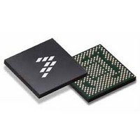
SC900841JVK Freescale Semiconductor, SC900841JVK Datasheet - Page 129

SC900841JVK
Manufacturer Part Number
SC900841JVK
Description
IC POWER MGT 338-MAPBGA
Manufacturer
Freescale Semiconductor
Specifications of SC900841JVK
Applications
PC's, PDA's
Operating Temperature
-40°C ~ 85°C
Mounting Type
Surface Mount
Package / Case
338-TBGA
Input Voltage
2.8 V to 4.4 V
Maximum Operating Temperature
+ 85 C
Minimum Operating Temperature
- 40 C
Lead Free Status / RoHS Status
Lead free / RoHS Compliant
Current - Supply
-
Voltage - Supply
-
Lead Free Status / Rohs Status
Lead free / RoHS Compliant
Available stocks
Company
Part Number
Manufacturer
Quantity
Price
Company:
Part Number:
SC900841JVK
Manufacturer:
Freescale Semiconductor
Quantity:
10 000
Company:
Part Number:
SC900841JVKR2
Manufacturer:
Freescale Semiconductor
Quantity:
10 000
- Current page: 129 of 192
- Download datasheet (8Mb)
Table 78. Charger Interrupt/Mask Registers Structure and Bits Description
Analog Integrated Circuit Device Data
Freescale Semiconductor
MUSBOVP
MUSBDET
MBATDET
SUSBOVP
SBATOVP
SUSBDET
SBATDET
MDCLMT
Reserved
SDCLMT
MCOMP
MTEMP
SCOMP
STEMP
2
3
4
5
6
7
0
1
2
3
4
5
6
7
Battery Over/Under-temperature Interrupt Signal Mask
x0 = Unmask
x1 = Mask
Battery Charge Cycle Completion Interrupt Signal Mask
x0 = Unmask
x1 = Mask
USB V
x0 = Unmask
x1 = Mask
Battery Detection Interrupt Signal Mask
x0 = Unmask
x1 = Mask
Charge Input Current Limit Detection Interrupt Signal Mask
x0 = Unmask
x1 = Mask
Charge Input Over-voltage Detection Interrupt Signal Mask
x0 = Unmask
x1 = Mask
Reserved
Battery Over-voltage Status
x0 = Battery voltage is lower than the limit (< V
x1 = Battery voltage is higher than the limit (> V
Battery temperature Status
x0 = Battery temperature is within valid window
x1 = Battery temperature is out of valid window
Battery Charge Cycle Completion Status
x0 = Charge cycle not complete (RDSTEN = 0), state not changed (RDSTEN = 1)
x1 = charge cycle complete (RDSTEN = 0), state changed (RDSTEN = 1)
Charger Input Voltage Status Signal
x0 = Charger input voltage not present (V
x1 = Charger input voltage present (V
Battery Present Status Signal
x0 = Battery not present (VBAT < VTRKL)
x1 = Battery present (VBAT > VTRKL)
Charge Input Current Limit Status
x0 = Charger input current is lower than the limit (< I
x1 = Charger input current is higher than the limit (> I
Charger Input Over-voltage Status
x0 = Charger input voltage is lower than the limit (< V
x1 = Charger input voltage is higher than the limit (> V
BUS
Detection Interrupt Signal Mask
SCHRGINT (ADDR 0xD2 - R - Default Value: 0x00)
RAWCHG
RAWCHG
> V
CHGCV
CHGCV
RAWCHGDET
< V
USBLMT
USBLMT
RAWCHGOVP
+ V
RAWCHGDET
RAWCHGOVP
+ V
BATTERY INTERFACE AND POWER PATH MANAGEMENT
OVRVOLT
OVRVOLT
)
)
)
)
)
)
)
)
FUNCTIONAL DEVICE OPERATION
900841
129
Related parts for SC900841JVK
Image
Part Number
Description
Manufacturer
Datasheet
Request
R
Part Number:
Description:
Manufacturer:
Freescale Semiconductor, Inc
Datasheet:
Part Number:
Description:
Manufacturer:
Freescale Semiconductor, Inc
Datasheet:
Part Number:
Description:
Manufacturer:
Freescale Semiconductor, Inc
Datasheet:
Part Number:
Description:
Manufacturer:
Freescale Semiconductor, Inc
Datasheet:
Part Number:
Description:
Manufacturer:
Freescale Semiconductor, Inc
Datasheet:
Part Number:
Description:
Manufacturer:
Freescale Semiconductor, Inc
Datasheet:
Part Number:
Description:
Manufacturer:
Freescale Semiconductor, Inc
Datasheet:
Part Number:
Description:
Manufacturer:
Freescale Semiconductor, Inc
Datasheet:
Part Number:
Description:
Manufacturer:
Freescale Semiconductor, Inc
Datasheet:
Part Number:
Description:
Manufacturer:
Freescale Semiconductor, Inc
Datasheet:
Part Number:
Description:
Manufacturer:
Freescale Semiconductor, Inc
Datasheet:
Part Number:
Description:
Manufacturer:
Freescale Semiconductor, Inc
Datasheet:
Part Number:
Description:
Manufacturer:
Freescale Semiconductor, Inc
Datasheet:
Part Number:
Description:
Manufacturer:
Freescale Semiconductor, Inc
Datasheet:
Part Number:
Description:
Manufacturer:
Freescale Semiconductor, Inc
Datasheet:


