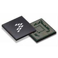
SC900841JVK Freescale Semiconductor, SC900841JVK Datasheet - Page 172

SC900841JVK
Manufacturer Part Number
SC900841JVK
Description
IC POWER MGT 338-MAPBGA
Manufacturer
Freescale Semiconductor
Specifications of SC900841JVK
Applications
PC's, PDA's
Operating Temperature
-40°C ~ 85°C
Mounting Type
Surface Mount
Package / Case
338-TBGA
Input Voltage
2.8 V to 4.4 V
Maximum Operating Temperature
+ 85 C
Minimum Operating Temperature
- 40 C
Lead Free Status / RoHS Status
Lead free / RoHS Compliant
Current - Supply
-
Voltage - Supply
-
Lead Free Status / Rohs Status
Lead free / RoHS Compliant
Available stocks
Company
Part Number
Manufacturer
Quantity
Price
Company:
Part Number:
SC900841JVK
Manufacturer:
Freescale Semiconductor
Quantity:
10 000
Company:
Part Number:
SC900841JVKR2
Manufacturer:
Freescale Semiconductor
Quantity:
10 000
- Current page: 172 of 192
- Download datasheet (8Mb)
Table 114. GPIO/GPOSW Register Structure and Bits Description
172
900841
FUNCTIONAL DEVICE OPERATION
GPIOS
DATAOUTx
GPIDBNCx 7:6
DATAINx
INTCTLx
GPIINT0
GPIINT1
GPIINT2
GPIINT3
Name
DRVx
DIRx
Bits
5:4
0
1
2
3
0
1
2
3
GPIOx Output Driver Type
x0 = Open Drain
x1 = CMOS
GPIOx Direction Configuration
x0 = Output (Type selected by Bit 0)
x1 = Input (Bit 0 is ignored)
The value in the DATA_IN bit reflects the electrical state of the GPIOx pin at the time the register read was initiated. When
Bit 1, DIRECTION, is 0 (Output Mode), the contents of this register are not required to be updated on reads and is assumed
to be invalid by the system controller. The PMIC should de-bounce the inputs over 1-10 ms to insure a clean transition.
X0 = Electrical Low
x1 = Electrical High
The value in the DATA_OUT bit reflects the desired electrical output state of the GPIOx pin. When Bit 1, DIRECTION, is 1
(Input Mode), the contents of this register may still be read or written, but will not be reflected until the GPIOx is reverted
to an output (Bit 1, DIRECTION, is 0)
x0 = Electrical Low
x1 = Electrical High (CMOS) or High-impedance Output (Open-Drain)
These bits set the interrupt definition. The MASK (00) determines if the corresponding interrupt flag bit is set or not on an
interrupt. The other logic levels will set the corresponding interrupt flag bit in the register upon the specific edge detection
defined by the level. They will also set bit 4 of the 1st level INTERRUPT register, see section Interrupt Controller for more
details.
x0 = Mask.
x1 = Negative Edge
x2 = Positive Edge
x3 = Both Edges
These bits set the debounce time on the GPIOx when configured as inputs
x0 = No Debounce
x1 = 10 ms
x2 = 20 ms
x3 = 30 ms
GPIO0 Interrupt Flag
x0 = No Interrupt occurred or Masked Interrupt
x1 = Interrupt occurred
GPIO1 Interrupt Flag
x0 = No Interrupt occurred or Masked Interrupt
x1 = Interrupt occurred
GPIO2 Interrupt Flag
x0 = No Interrupt occurred or Masked Interrupt
x1 = Interrupt occurred
GPIO3 Interrupt Flag
x0 = No Interrupt occurred or Masked Interrupt
x1 = Interrupt occurred
(35)
(34)
(34)
(34)
GPIOINT (ADDR 0xE8 - R - Default Value: 0x00)
GPIOCNTLx (x = 0 to 7)
Description
(34)
Analog Integrated Circuit Device Data
Freescale Semiconductor
Related parts for SC900841JVK
Image
Part Number
Description
Manufacturer
Datasheet
Request
R
Part Number:
Description:
Manufacturer:
Freescale Semiconductor, Inc
Datasheet:
Part Number:
Description:
Manufacturer:
Freescale Semiconductor, Inc
Datasheet:
Part Number:
Description:
Manufacturer:
Freescale Semiconductor, Inc
Datasheet:
Part Number:
Description:
Manufacturer:
Freescale Semiconductor, Inc
Datasheet:
Part Number:
Description:
Manufacturer:
Freescale Semiconductor, Inc
Datasheet:
Part Number:
Description:
Manufacturer:
Freescale Semiconductor, Inc
Datasheet:
Part Number:
Description:
Manufacturer:
Freescale Semiconductor, Inc
Datasheet:
Part Number:
Description:
Manufacturer:
Freescale Semiconductor, Inc
Datasheet:
Part Number:
Description:
Manufacturer:
Freescale Semiconductor, Inc
Datasheet:
Part Number:
Description:
Manufacturer:
Freescale Semiconductor, Inc
Datasheet:
Part Number:
Description:
Manufacturer:
Freescale Semiconductor, Inc
Datasheet:
Part Number:
Description:
Manufacturer:
Freescale Semiconductor, Inc
Datasheet:
Part Number:
Description:
Manufacturer:
Freescale Semiconductor, Inc
Datasheet:
Part Number:
Description:
Manufacturer:
Freescale Semiconductor, Inc
Datasheet:
Part Number:
Description:
Manufacturer:
Freescale Semiconductor, Inc
Datasheet:


