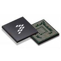
SC900841JVK Freescale Semiconductor, SC900841JVK Datasheet - Page 174

SC900841JVK
Manufacturer Part Number
SC900841JVK
Description
IC POWER MGT 338-MAPBGA
Manufacturer
Freescale Semiconductor
Specifications of SC900841JVK
Applications
PC's, PDA's
Operating Temperature
-40°C ~ 85°C
Mounting Type
Surface Mount
Package / Case
338-TBGA
Input Voltage
2.8 V to 4.4 V
Maximum Operating Temperature
+ 85 C
Minimum Operating Temperature
- 40 C
Lead Free Status / RoHS Status
Lead free / RoHS Compliant
Current - Supply
-
Voltage - Supply
-
Lead Free Status / Rohs Status
Lead free / RoHS Compliant
Available stocks
Company
Part Number
Manufacturer
Quantity
Price
Company:
Part Number:
SC900841JVK
Manufacturer:
Freescale Semiconductor
Quantity:
10 000
Company:
Part Number:
SC900841JVKR2
Manufacturer:
Freescale Semiconductor
Quantity:
10 000
- Current page: 174 of 192
- Download datasheet (8Mb)
Table 115. GPO Register Structure and Bits Description
OVERVIEW
the write enable bit, 10-bit address and 5 "dead" bits between
the data and address fields. The next 8 bits are the data bits.
The one write enable bit selects whether the SPI transaction
is a read or a write.
data bits each. The map is not fully populated. A summarized
structure of the register set is given in the following tables.
Expanded bit descriptions are included in the individual
functional sections for application guidance.
SPI BIT MAP
• Block: This corresponds directly to the chapter, section or
• Address: The register memory map address allocation in
• Register Name
• R/W: Defines if the register is a Read/Write register or only
Table 116. SPI Register Map
174
900841
FUNCTIONAL DEVICE OPERATION
SPI REGISTER MAP
GPO2
GPO3
GPO4
GPO5
GPO6
GPO7
Block
Chip1
Chip2
Chip3
Chip4
The SPI frame is organized as 24 bits. The first 16 bits is
The addressable register map spans 1024 registers of 8
The tables include the following fields:
topic in which the detailed register description is included.
HEX format
a Read register
Address
0x00
0x01
0x02
0x03
2
3
4
5
6
7
Register Name
GPO2 Output Level
x0 = Low
x1 = High (To voltage supplied on GPOVCC Pin)
GPO3 Output Level
x0 = Low
x1 = High (To voltage supplied on GPOVCC Pin)
GPO4 Output Level
x0 = Low
x1 = High (To voltage supplied on GPOVCC Pin)
GPO5 Output Level
x0 = Low
x1 = High (To voltage supplied on GPOVCC Pin)
GPO6 Output Level
x0 = Low
x1 = High (To voltage supplied on GPOVCC Pin)
GPO7 Output Level
x0 = Low
x1 = High (To voltage supplied on GPOVCC Pin)
ID1
ID2
ID3
ID4
R/W
R
R
R
R
RSVD
RSVD
RSVD
RSVD
D7
RSVD
RSVD
RSVD
RSVD
D6
SPI REGISTER MAP
RSVD
RSVD
D5
REV1[2:0]
REV2[2:0]
RSVD
RSVD
D4
• D7-D0: The 8-bit data included in the register with each
• Initial: The register's default value after power up
• Function: A short description of the register's function
• Reserved registers/bits are not implemented in the design
• Registers under the "FSL" block are Freescale dedicated
• Registers under the "VD2" and "VD3" blocks are blocked
• The table only displays up to address 0x2FF. Address
bit's name and location within the field included
Some important notes about data in the table:
and they will always read as a 0
registers and are not defined in the customer
specifications. These registers represent additional
functionality that Freescale is offering to enhance the
performance of the overall system
from being used by Freescale
space between 0x300 and 0x3FF is reserved for future
application use. Freescale is currently using the 0x300 to
0x3FF space for test and debug register implementation.
This will not effect the application or any future use plans
for this address space. The details of this space
implementation are not discussed in this document.
RSVD
RSVD
D3
RSVD
RSVD
D2
VENDID1[2:0]
VENDID2[2:0]
Analog Integrated Circuit Device Data
RSVD
RSVD
D1
RSVD
RSVD
Freescale Semiconductor
D0
Initial
0x38 Chip1 ID
0x00 Chip2 ID
0x00 Chip3 ID
0x00 Chip4 ID
Function
Related parts for SC900841JVK
Image
Part Number
Description
Manufacturer
Datasheet
Request
R
Part Number:
Description:
Manufacturer:
Freescale Semiconductor, Inc
Datasheet:
Part Number:
Description:
Manufacturer:
Freescale Semiconductor, Inc
Datasheet:
Part Number:
Description:
Manufacturer:
Freescale Semiconductor, Inc
Datasheet:
Part Number:
Description:
Manufacturer:
Freescale Semiconductor, Inc
Datasheet:
Part Number:
Description:
Manufacturer:
Freescale Semiconductor, Inc
Datasheet:
Part Number:
Description:
Manufacturer:
Freescale Semiconductor, Inc
Datasheet:
Part Number:
Description:
Manufacturer:
Freescale Semiconductor, Inc
Datasheet:
Part Number:
Description:
Manufacturer:
Freescale Semiconductor, Inc
Datasheet:
Part Number:
Description:
Manufacturer:
Freescale Semiconductor, Inc
Datasheet:
Part Number:
Description:
Manufacturer:
Freescale Semiconductor, Inc
Datasheet:
Part Number:
Description:
Manufacturer:
Freescale Semiconductor, Inc
Datasheet:
Part Number:
Description:
Manufacturer:
Freescale Semiconductor, Inc
Datasheet:
Part Number:
Description:
Manufacturer:
Freescale Semiconductor, Inc
Datasheet:
Part Number:
Description:
Manufacturer:
Freescale Semiconductor, Inc
Datasheet:
Part Number:
Description:
Manufacturer:
Freescale Semiconductor, Inc
Datasheet:


