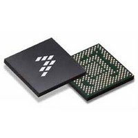
SC900841JVK Freescale Semiconductor, SC900841JVK Datasheet - Page 169

SC900841JVK
Manufacturer Part Number
SC900841JVK
Description
IC POWER MGT 338-MAPBGA
Manufacturer
Freescale Semiconductor
Specifications of SC900841JVK
Applications
PC's, PDA's
Operating Temperature
-40°C ~ 85°C
Mounting Type
Surface Mount
Package / Case
338-TBGA
Input Voltage
2.8 V to 4.4 V
Maximum Operating Temperature
+ 85 C
Minimum Operating Temperature
- 40 C
Lead Free Status / RoHS Status
Lead free / RoHS Compliant
Current - Supply
-
Voltage - Supply
-
Lead Free Status / Rohs Status
Lead free / RoHS Compliant
Available stocks
Company
Part Number
Manufacturer
Quantity
Price
Company:
Part Number:
SC900841JVK
Manufacturer:
Freescale Semiconductor
Quantity:
10 000
Company:
Part Number:
SC900841JVKR2
Manufacturer:
Freescale Semiconductor
Quantity:
10 000
Table 112. Extended ADC Control Register Structure and Bits Description
DESCRIPTION
switches, and eight GPOs for platform control.
OD signaling levels, based on the voltage level on the
GPIOVCC and GPOSWVCC. The GPOs shall support
CMOS signaling levels, based on the voltage level on the
GPOVCC pin. As inputs, they need to be 3.6 V tolerant and
should be de-bounced for a period of no more than 10 ms
minimum.
GPIO inputs/outputs, GPIO[7:0] for general purpose sensing
and platform control. Only GPIOs support an input function.
whose primary function will be to serve as gating signals for
discrete platform VR switches.
They are designed to support dynamic gating of sub-circuits
from a main well or always on supply, and therefore require
additional attention when switching. Specifically, GPOSWs
must implement slew rate control to prevent dangerously high
instantaneous inrush currents to previously isolated rails. For
Analog Integrated Circuit Device Data
Freescale Semiconductor
ONEC[14:8]
ONEC[7:0]
CCFAULT
RAWCCH
Reserved
RAWCCL
The 900841 has eight GPIOs, four GPOSWs for platform
As outputs, the GPIOs and GPOSWs shall support CMOS/
The 900841 will provide one bank of eight configurable
The PMIC shall provide one bank of four GPOSW outputs,
GPOSW outputs vary from GPIOs in an important way.
Table 113. GPIOs Capabilities and Default States
GPIO0
GPIO1
GPIO2
GPIO3
GPIO4
GPIO5
GPIO6
GPIO7
GPIO
7:0
6:0
7:0
7:0
7
7
Charging Overflow Status Bit
x0 = Coulomb Counter Reading is < Positive 32767
x1 = Coulomb Counter Reading is > Positive 32767
8 LSBs of ONEC[14:0] internal register
7 MSBs of ONEC[14:0] internal register
Reserved
8 MSBs CCOUT Raw Data
8 LSBs of CCOUT Raw Data
Input
Yes
Yes
Yes
Yes
Yes
Yes
Yes
Yes
ONECLREG (ADDR 0x1E0 - R/W -Default Value: 0x1A)
ONECHREG (ADDR 0x1E1 - R/W -Default Value: 0x00)
RAWCCL (ADDR 0x1E3 - R/W - Default Value: 0x00)
RAWCCH (ADDR 0x1E2 - R/W - Default Value: 0x00
Output
Yes
Yes
Yes
Yes
Yes
Yes
Yes
Yes
CMOS
Yes
Yes
Yes
Yes
Yes
Yes
Yes
Yes
GPIOS
Yes
Yes
Yes
Yes
Yes
Yes
Yes
Yes
OD
CMOS configured outputs, slew rate control will be specified
in terms of output resistance at the GPOSW output pin. When
operating as an open drain output, the slew rate specification
is the same, but will be interpreted assuming an externally
connected 100 kΩ (±1%) pull-up resistance.
between a high-impedance (>1.0 MΩ) state and a low-
impedance (20 Ω nominal) state when operating in open
drain mode. When operating in CMOS mode, the outputs are
expected to drive from the voltage supplied on the GPIOVCC
pin with a 20 Ω output drive capability (for GPIOs) or
GPOSWVCC pin (for GPOSWs).
therefore be specified as relative percentages of the driving
supply.
board.
drain, the pull-up voltage cannot exceed that of the
GPIOVCC and GPOSWVCC voltage level respectively.
and their capabilities.
Both GPIOs and GPOSWs are expected to switch
The electrical characteristics of the output buffer will
Any unused GPIO pin should be tied to ground on the
When any GPIO or GPOSW pin is configured as an open
Table 113
Slew CNTL
No
No
No
No
No
No
No
No
shows the default state of the different GPIOs
Default Mode
Input
Input
Input
Input
Input
Input
Input
Input
FUNCTIONAL DEVICE OPERATION
Default Level
HI-Z
HI-Z
HI-Z
HI-Z
HI-Z
HI-Z
HI-Z
HI-Z
GPIOS
900841
169


