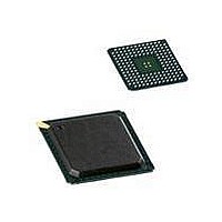
LPC1850FET256,551 NXP Semiconductors, LPC1850FET256,551 Datasheet - Page 32

LPC1850FET256,551
Manufacturer Part Number
LPC1850FET256,551
Description
MCU 32BIT ARM CORTEX M3 256BGA
Manufacturer
NXP Semiconductors
Series
LPC18xxr
Datasheet
1.LPC1830FET256551.pdf
(87 pages)
Specifications of LPC1850FET256,551
Core Processor
ARM® Cortex-M3™
Core Size
32-Bit
Speed
150MHz
Connectivity
CAN, EBI/EMI, Ethernet, I²C, IrDA, Microwire, QEI, SD/MMC, SPI, SSI, SSP, UART/USART, USB, USB OTG
Peripherals
Brown-out Detect/Reset, DMA, I²S, LCD, POR, PWM, WDT
Number Of I /o
80
Program Memory Size
-
Program Memory Type
ROMless
Eeprom Size
-
Ram Size
200K x 8
Voltage - Supply (vcc/vdd)
2.2 V ~ 3.6 V
Data Converters
A/D 8x10b; D/A 1x10b
Oscillator Type
Internal
Operating Temperature
-40°C ~ 85°C
Package / Case
256-LBGA
Processor Series
LPC1850
Core
ARM Cortex M3
Data Bus Width
32 bit
Data Ram Size
200 KB
Interface Type
SPI Flash (SPIFI), USB, Ethernet, LCD, External Memory Controller, I2C
Maximum Clock Frequency
150 MHz
Number Of Programmable I/os
80
Number Of Timers
6
Operating Supply Voltage
2 V to 3.6 V
Maximum Operating Temperature
+ 85 C
Mounting Style
SMD/SMT
Minimum Operating Temperature
- 40 C
Operating Temperature Range
- 40 C to + 85 C
Lead Free Status / Rohs Status
Lead free / RoHS Compliant
Other names
568-6682
Available stocks
Company
Part Number
Manufacturer
Quantity
Price
Company:
Part Number:
LPC1850FET256,551
Manufacturer:
NXP Semiconductors
Quantity:
10 000
Part Number:
LPC1850FET256,551
Manufacturer:
NXP/恩智浦
Quantity:
20 000
NXP Semiconductors
LPC1850_30_20_10
Objective data sheet
7.4.2 Interrupt sources
7.5 Event router
7.6 System Tick timer (SysTick)
7.7 On-chip static RAM
7.8 Boot ROM
Each peripheral device has one interrupt line connected to the NVIC but may have several
interrupt flags. Individual interrupt flags may also represent more than one interrupt
source.
The event router combines various internal signals, interrupts, and the external interrupt
pins (WAKEUP[3:0]) to create an interrupt in the NVIC if enabled and to create a wake-up
signal to the ARM core and the CCU for waking up from Sleep, Deep-sleep, Power-down,
and Deep power-down modes. Individual events can be configured as edge or level
sensitive and can be enabled or disabled in the event router. The event router can be
battery powered.
The following events if enabled in the event router can create a wake-up signal and/or an
interrupt:
The ARM Cortex-M3 includes a system tick timer (SYSTICK) that is intended to generate
a dedicated SYSTICK exception at a 10 ms interval.
The LPC1850/30/20/10 support up to 200 kB SRAM with separate bus master access for
higher throughput and individual power control for low power operation.
The internal ROM memory is used to store the boot code of the LPC1850/30/20/10. After
a reset, the ARM processor will start its code execution from this memory.
The boot ROM memory includes the following features:
AES capable parts also support:
•
•
•
•
•
•
•
•
•
•
•
External pins WAKEUP0/1/2/3 and RESET
Alarm timer, RTC, WWDT, BOD interrupts
C_CAN and QEI interrupts
Ethernet, USB0, USB1 signals
Selected outputs of combined timers (SCT and timer0/1/3)
ROM memory size is 32 kB.
Supports booting from UART interfaces and external static memory such as NOR
flash, SPI flash, quad SPI flash.
Includes APIs for power control and OTP programming.
Includes SPIFI drivers.
Includes a flexible USB device stack that supports Human Interface Device (HID),
Mass Storage Class (MSC), and Device Firmware Upgrade (DFU) drivers.
CMAC authentication on the boot image.
All information provided in this document is subject to legal disclaimers.
Rev. 1.2 — 17 February 2011
32-bit ARM Cortex-M3 microcontroller
LPC1850/30/20/10
© NXP B.V. 2011. All rights reserved.
32 of 87


