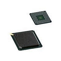
LPC1850FET256,551 NXP Semiconductors, LPC1850FET256,551 Datasheet - Page 65

LPC1850FET256,551
Manufacturer Part Number
LPC1850FET256,551
Description
MCU 32BIT ARM CORTEX M3 256BGA
Manufacturer
NXP Semiconductors
Series
LPC18xxr
Datasheet
1.LPC1830FET256551.pdf
(87 pages)
Specifications of LPC1850FET256,551
Core Processor
ARM® Cortex-M3™
Core Size
32-Bit
Speed
150MHz
Connectivity
CAN, EBI/EMI, Ethernet, I²C, IrDA, Microwire, QEI, SD/MMC, SPI, SSI, SSP, UART/USART, USB, USB OTG
Peripherals
Brown-out Detect/Reset, DMA, I²S, LCD, POR, PWM, WDT
Number Of I /o
80
Program Memory Size
-
Program Memory Type
ROMless
Eeprom Size
-
Ram Size
200K x 8
Voltage - Supply (vcc/vdd)
2.2 V ~ 3.6 V
Data Converters
A/D 8x10b; D/A 1x10b
Oscillator Type
Internal
Operating Temperature
-40°C ~ 85°C
Package / Case
256-LBGA
Processor Series
LPC1850
Core
ARM Cortex M3
Data Bus Width
32 bit
Data Ram Size
200 KB
Interface Type
SPI Flash (SPIFI), USB, Ethernet, LCD, External Memory Controller, I2C
Maximum Clock Frequency
150 MHz
Number Of Programmable I/os
80
Number Of Timers
6
Operating Supply Voltage
2 V to 3.6 V
Maximum Operating Temperature
+ 85 C
Mounting Style
SMD/SMT
Minimum Operating Temperature
- 40 C
Operating Temperature Range
- 40 C to + 85 C
Lead Free Status / Rohs Status
Lead free / RoHS Compliant
Other names
568-6682
Available stocks
Company
Part Number
Manufacturer
Quantity
Price
Company:
Part Number:
LPC1850FET256,551
Manufacturer:
NXP Semiconductors
Quantity:
10 000
Part Number:
LPC1850FET256,551
Manufacturer:
NXP/恩智浦
Quantity:
20 000
NXP Semiconductors
Table 13.
[1]
[2]
[3]
[4]
LPC1850_30_20_10
Objective data sheet
Symbol
T
T
SSP master
t
t
t
t
SSP slave
t
t
t
t
DS
DH
v(Q)
h(Q)
DS
DH
v(Q)
h(Q)
cy(PCLK)
cy(clk)
T
main clock frequency f
register), and the SSP CPSDVSR parameter (specified in the SSP clock prescale register).
T
T
T
cy(clk)
amb
cy(clk)
amb
= 40 C to 85 C; V
= 25 C; V
= (SSPCLKDIV (1 + SCR) CPSDVSR) / f
= 12 T
Dynamic characteristics: SSP pins in SPI mode
Parameter
PCLK cycle time
clock cycle time
data set-up time
data hold time
data output valid time
data output hold time
data set-up time
data hold time
data output valid time
data output hold time
11.4 SSP interface
cy(PCLK)
DD(REG)(3V3)
main
.
DD(REG)(3V3)
, the SSP peripheral clock divider (SSPCLKDIV), the SSP SCR parameter (specified in the SSP0CR0
= 3.3 V; V
DD(IO)
= 2.0 V to 3.6 V; V
All information provided in this document is subject to legal disclaimers.
= 3.3 V.
Conditions
in SPI mode
in SPI mode
in SPI mode
in SPI mode
in SPI mode
in SPI mode
in SPI mode
in SPI mode
Rev. 1.2 — 17 February 2011
main
. The clock cycle time derived from the SPI bit rate T
DD(IO)
= 2.0 V to 3.6 V.
[1]
[2]
[2]
[2]
[2]
[3][4]
[3][4]
[3][4]
[3][4]
Min
<tbd>
<tbd>
<tbd>
-
-
-
<tbd>
<tbd> T
<tbd>
-
-
32-bit ARM Cortex-M3 microcontroller
cy(PCLK)
LPC1850/30/20/10
+
Max
-
-
T
<tbd>
<tbd>
<tbd>
-
-
<tbd> T
<tbd>
<tbd> T
<tbd>
cy(clk)
cy(clk)
cy(PCLK)
cy(PCLK)
© NXP B.V. 2011. All rights reserved.
is a function of the
+
+
Unit
ns
ns
ns
ns
ns
ns
ns
ns
ns
ns
65 of 87


