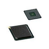
LPC1850FET256,551 NXP Semiconductors, LPC1850FET256,551 Datasheet - Page 48

LPC1850FET256,551
Manufacturer Part Number
LPC1850FET256,551
Description
MCU 32BIT ARM CORTEX M3 256BGA
Manufacturer
NXP Semiconductors
Series
LPC18xxr
Datasheet
1.LPC1830FET256551.pdf
(87 pages)
Specifications of LPC1850FET256,551
Core Processor
ARM® Cortex-M3™
Core Size
32-Bit
Speed
150MHz
Connectivity
CAN, EBI/EMI, Ethernet, I²C, IrDA, Microwire, QEI, SD/MMC, SPI, SSI, SSP, UART/USART, USB, USB OTG
Peripherals
Brown-out Detect/Reset, DMA, I²S, LCD, POR, PWM, WDT
Number Of I /o
80
Program Memory Size
-
Program Memory Type
ROMless
Eeprom Size
-
Ram Size
200K x 8
Voltage - Supply (vcc/vdd)
2.2 V ~ 3.6 V
Data Converters
A/D 8x10b; D/A 1x10b
Oscillator Type
Internal
Operating Temperature
-40°C ~ 85°C
Package / Case
256-LBGA
Processor Series
LPC1850
Core
ARM Cortex M3
Data Bus Width
32 bit
Data Ram Size
200 KB
Interface Type
SPI Flash (SPIFI), USB, Ethernet, LCD, External Memory Controller, I2C
Maximum Clock Frequency
150 MHz
Number Of Programmable I/os
80
Number Of Timers
6
Operating Supply Voltage
2 V to 3.6 V
Maximum Operating Temperature
+ 85 C
Mounting Style
SMD/SMT
Minimum Operating Temperature
- 40 C
Operating Temperature Range
- 40 C to + 85 C
Lead Free Status / Rohs Status
Lead free / RoHS Compliant
Other names
568-6682
Available stocks
Company
Part Number
Manufacturer
Quantity
Price
Company:
Part Number:
LPC1850FET256,551
Manufacturer:
NXP Semiconductors
Quantity:
10 000
Part Number:
LPC1850FET256,551
Manufacturer:
NXP/恩智浦
Quantity:
20 000
NXP Semiconductors
LPC1850_30_20_10
Objective data sheet
7.14.5.1 Features
7.15.1.1 Features
7.15.2.1 Features
7.14.5 Windowed WatchDog Timer (WWDT)
7.15.1 Analog-to-Digital Converter (ADC0/1)
7.15.2 Digital-to-Analog Converter (DAC)
7.15 Analog peripherals
The purpose of the watchdog is to reset the controller if software fails to periodically
service it within a programmable time window.
•
•
•
•
•
•
•
•
•
•
•
•
•
•
•
•
•
•
•
•
32-bit compare mask. An interrupt is generated when the counter value equals the
compare value, after masking. This allows for combinations not possible with a simple
compare.
Internally resets chip if not periodically reloaded during the programmable time-out
period.
Optional windowed operation requires reload to occur between a minimum and
maximum time period, both programmable.
Optional warning interrupt can be generated at a programmable time prior to
watchdog time-out.
Enabled by software but requires a hardware reset or a watchdog reset/interrupt to be
disabled.
Incorrect feed sequence causes reset or interrupt if enabled.
Flag to indicate watchdog reset.
Programmable 24-bit timer with internal prescaler.
Selectable time period from (T
multiples of T
The Watchdog Clock (WDCLK) uses the IRC as the clock source.
10-bit successive approximation analog to digital converter.
Input multiplexing among 8 pins.
Power-down mode.
Measurement range 0 to 3 V.
Sampling frequency up to 400 kSamples/s.
Burst conversion mode for single or multiple inputs.
Optional conversion on transition on ADCTRIG0 or ADCTRIG1 pins, combined timer
outputs 8 or 15, or the PWM output MCOA2.
Individual result registers for each A/D channel to reduce interrupt overhead.
DMA support.
10-bit resolution
All information provided in this document is subject to legal disclaimers.
cy(WDCLK)
Rev. 1.2 — 17 February 2011
4.
cy(WDCLK)
256 4) to (T
32-bit ARM Cortex-M3 microcontroller
LPC1850/30/20/10
cy(WDCLK)
2
© NXP B.V. 2011. All rights reserved.
24
4) in
48 of 87


