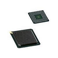
LPC1850FET256,551 NXP Semiconductors, LPC1850FET256,551 Datasheet - Page 45

LPC1850FET256,551
Manufacturer Part Number
LPC1850FET256,551
Description
MCU 32BIT ARM CORTEX M3 256BGA
Manufacturer
NXP Semiconductors
Series
LPC18xxr
Datasheet
1.LPC1830FET256551.pdf
(87 pages)
Specifications of LPC1850FET256,551
Core Processor
ARM® Cortex-M3™
Core Size
32-Bit
Speed
150MHz
Connectivity
CAN, EBI/EMI, Ethernet, I²C, IrDA, Microwire, QEI, SD/MMC, SPI, SSI, SSP, UART/USART, USB, USB OTG
Peripherals
Brown-out Detect/Reset, DMA, I²S, LCD, POR, PWM, WDT
Number Of I /o
80
Program Memory Size
-
Program Memory Type
ROMless
Eeprom Size
-
Ram Size
200K x 8
Voltage - Supply (vcc/vdd)
2.2 V ~ 3.6 V
Data Converters
A/D 8x10b; D/A 1x10b
Oscillator Type
Internal
Operating Temperature
-40°C ~ 85°C
Package / Case
256-LBGA
Processor Series
LPC1850
Core
ARM Cortex M3
Data Bus Width
32 bit
Data Ram Size
200 KB
Interface Type
SPI Flash (SPIFI), USB, Ethernet, LCD, External Memory Controller, I2C
Maximum Clock Frequency
150 MHz
Number Of Programmable I/os
80
Number Of Timers
6
Operating Supply Voltage
2 V to 3.6 V
Maximum Operating Temperature
+ 85 C
Mounting Style
SMD/SMT
Minimum Operating Temperature
- 40 C
Operating Temperature Range
- 40 C to + 85 C
Lead Free Status / Rohs Status
Lead free / RoHS Compliant
Other names
568-6682
Available stocks
Company
Part Number
Manufacturer
Quantity
Price
Company:
Part Number:
LPC1850FET256,551
Manufacturer:
NXP Semiconductors
Quantity:
10 000
Part Number:
LPC1850FET256,551
Manufacturer:
NXP/恩智浦
Quantity:
20 000
NXP Semiconductors
LPC1850_30_20_10
Objective data sheet
7.13.4.1 Features
7.13.5.1 Features
7.13.5 I
The I
The I
and one word select signal. The basic I
always the master, and one slave. The I
receive channel, each of which can operate as either a master or a slave.
2
•
•
•
•
•
•
•
•
•
•
•
•
•
•
•
•
•
•
•
•
•
S interface
I
supports Fast mode plus with bit rates up to 1 Mbit/s.
I
Easy to configure as master, slave, or master/slave.
Programmable clocks allow versatile rate control.
Bidirectional data transfer between masters and slaves.
Multi-master bus (no central master).
Arbitration between simultaneously transmitting masters without corruption of serial
data on the bus.
Serial clock synchronization allows devices with different bit rates to communicate via
one serial bus.
Serial clock synchronization can be used as a handshake mechanism to suspend and
resume serial transfer.
The I
All I
The interface has separate input/output channels each of which can operate in master
or slave mode.
Capable of handling 8-bit, 16-bit, and 32-bit word sizes.
Mono and stereo audio data supported.
The sampling frequency can range from 16 kHz to 96 kHz (16, 22.05, 32, 44.1, 48,
96) kHz.
Support for an audio master clock.
Configurable word select period in master mode (separately for I
output).
Two 8-word FIFO data buffers are provided, one for transmit and one for receive.
Generates interrupt requests when buffer levels cross a programmable boundary.
Two DMA requests, controlled by programmable buffer levels. These are connected
to the GPDMA block.
Controls include reset, stop and mute options separately for I
output.
2
2
2
2
C0 is a standard I
C1 uses standard I/O pins with bit rates of up to 400 kbit/s (Fast I
S-bus provides a standard communication interface for digital audio applications.
S-bus specification defines a 3-wire serial bus using one data line, one clock line,
2
C-bus controllers support multiple address recognition and a bus monitor mode.
2
C-bus can be used for test and diagnostic purposes.
All information provided in this document is subject to legal disclaimers.
Rev. 1.2 — 17 February 2011
2
C compliant bus interface with open-drain pins. I
2
2
S-bus connection has one master, which is
S-bus interface provides a separate transmit and
32-bit ARM Cortex-M3 microcontroller
LPC1850/30/20/10
2
S-bus input and I
2
S-bus input and
2
© NXP B.V. 2011. All rights reserved.
C-bus).
2
C0 also
2
45 of 87
S-bus


