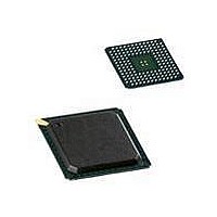
LPC1850FET256,551 NXP Semiconductors, LPC1850FET256,551 Datasheet - Page 9

LPC1850FET256,551
Manufacturer Part Number
LPC1850FET256,551
Description
MCU 32BIT ARM CORTEX M3 256BGA
Manufacturer
NXP Semiconductors
Series
LPC18xxr
Datasheet
1.LPC1830FET256551.pdf
(87 pages)
Specifications of LPC1850FET256,551
Core Processor
ARM® Cortex-M3™
Core Size
32-Bit
Speed
150MHz
Connectivity
CAN, EBI/EMI, Ethernet, I²C, IrDA, Microwire, QEI, SD/MMC, SPI, SSI, SSP, UART/USART, USB, USB OTG
Peripherals
Brown-out Detect/Reset, DMA, I²S, LCD, POR, PWM, WDT
Number Of I /o
80
Program Memory Size
-
Program Memory Type
ROMless
Eeprom Size
-
Ram Size
200K x 8
Voltage - Supply (vcc/vdd)
2.2 V ~ 3.6 V
Data Converters
A/D 8x10b; D/A 1x10b
Oscillator Type
Internal
Operating Temperature
-40°C ~ 85°C
Package / Case
256-LBGA
Processor Series
LPC1850
Core
ARM Cortex M3
Data Bus Width
32 bit
Data Ram Size
200 KB
Interface Type
SPI Flash (SPIFI), USB, Ethernet, LCD, External Memory Controller, I2C
Maximum Clock Frequency
150 MHz
Number Of Programmable I/os
80
Number Of Timers
6
Operating Supply Voltage
2 V to 3.6 V
Maximum Operating Temperature
+ 85 C
Mounting Style
SMD/SMT
Minimum Operating Temperature
- 40 C
Operating Temperature Range
- 40 C to + 85 C
Lead Free Status / Rohs Status
Lead free / RoHS Compliant
Other names
568-6682
Available stocks
Company
Part Number
Manufacturer
Quantity
Price
Company:
Part Number:
LPC1850FET256,551
Manufacturer:
NXP Semiconductors
Quantity:
10 000
Part Number:
LPC1850FET256,551
Manufacturer:
NXP/恩智浦
Quantity:
20 000
NXP Semiconductors
Table 3.
LPC1850_30_20_10
Objective data sheet
Symbol
P1_18
P1_19
P1_20
P2_0
P2_1
P2_2
P2_3
P2_4
[2]
[2]
[2]
[2]
[2]
[2]
[2]
[2]
Pin description
N12
M11 I; PU
M10 I; PU
T16
N15
M15 I; PU
J12
K11
…continued
Reset
state
[1]
I; PU
I; PU
I; PU
I; PU
I; PU
Type Description
I/O
I/O
-
O
I
I/O
-
-
I/O
I/O
-
O
-
O
I/O
O
-
I
I/O
O
-
I/O
I/O
O
-
I/O
O
I
-
I/O
I
I
All information provided in this document is subject to legal disclaimers.
GPIO0[13] — General purpose digital input/output pin.
U2_DIR — RS-485/EIA-485 output enable/direction control for UART2.
n.c.
ENET_TXD0 — Ethernet transmit data 0 (RMII/MII interface).
ENET_TX_CLK (ENET_REF_CLK) — Ethernet Transmit Clock (MII
interface) or Ethernet Reference Clock (RMII interface).
SSP1_SCK — Serial clock for SSP1.
n.c.
n.c.
GPIO0[15] — General purpose digital input/output pin.
SSP1_SSEL — Slave Select for SSP1.
n.c.
ENET_TXD1 — Ethernet transmit data 1 (RMII/MII interface).
n.c.
U0_TXD — Transmitter output for USART0.
EXTBUS_A13 — External memory address line 13.
USB0_PWR_EN — VBUS drive signal (towards external charge pump or
power management unit); indicates that Vbus must be driven (active high).
n.c.
U0_RXD — Receiver input for USART0.
EXTBUS_A12 — External memory address line 12.
USB0_PWR_FAULT — Port power fault signal indicating overcurrent
condition; this signal monitors over-current on the USB bus (external circuitry
required to detect over-current condition).
n.c.
U0_UCLK — Serial clock input/output for USART0 in synchronous mode.
EXTBUS_A11 — External memory address line 11.
USB0_IND1 — USB0 port indicator LED control output 1.
n.c.
I2C1_SDA — I
pad).
U3_TXD — Transmitter output for USART3.
CTIN_1 — SCT input 1. Capture input 1 of timer 0. Capture input 1 of timer 2.
n.c.
I2C1_SCL — I
pad).
U3_RXD — Receiver input for USART3.
CTIN_0 — SCT input 0. Capture input 0 of timer 0, 1, 2, 3.
Rev. 1.2 — 17 February 2011
2
2
C1 clock input/output (this pin does not use a specialized I
C1 data input/output (this pin does not use a specialized I
32-bit ARM Cortex-M3 microcontroller
LPC1850/30/20/10
© NXP B.V. 2011. All rights reserved.
9 of 87
2
2
C
C


