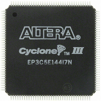
EP3C5E144I7N Altera, EP3C5E144I7N Datasheet - Page 132

EP3C5E144I7N
Manufacturer Part Number
EP3C5E144I7N
Description
IC CYCLONE III FPGA 5K 144 EQFP
Manufacturer
Altera
Series
Cyclone® IIIr
Datasheets
1.EP3C5F256C8N.pdf
(5 pages)
2.EP3C5F256C8N.pdf
(34 pages)
3.EP3C5F256C8N.pdf
(66 pages)
4.EP3C5F256C8N.pdf
(14 pages)
5.EP3C5F256C8N.pdf
(76 pages)
6.EP3C5E144I7N.pdf
(274 pages)
Specifications of EP3C5E144I7N
Number Of Logic Elements/cells
5136
Number Of Labs/clbs
321
Total Ram Bits
423936
Number Of I /o
94
Voltage - Supply
1.15 V ~ 1.25 V
Mounting Type
Surface Mount
Operating Temperature
-40°C ~ 100°C
Package / Case
144-EQFP
Family Name
Cyclone III
Number Of Logic Blocks/elements
5136
# I/os (max)
94
Frequency (max)
437.5MHz
Process Technology
65nm
Operating Supply Voltage (typ)
1.2V
Logic Cells
5136
Ram Bits
423936
Operating Supply Voltage (min)
1.15V
Operating Supply Voltage (max)
1.25V
Operating Temp Range
-40C to 100C
Operating Temperature Classification
Industrial
Mounting
Surface Mount
Pin Count
144
Package Type
EQFP
For Use With
544-2601 - KIT DEV CYCLONE III LS EP3CLS200544-2411 - KIT DEV NIOS II CYCLONE III ED.
Lead Free Status / RoHS Status
Lead free / RoHS Compliant
Number Of Gates
-
Lead Free Status / Rohs Status
Compliant
Other names
544-2557
Available stocks
Company
Part Number
Manufacturer
Quantity
Price
Company:
Part Number:
EP3C5E144I7N
Manufacturer:
Altera
Quantity:
135
Company:
Part Number:
EP3C5E144I7N
Manufacturer:
ALTERA32
Quantity:
345
Part Number:
EP3C5E144I7N
Manufacturer:
ALTERA/阿尔特拉
Quantity:
20 000
7–8
Figure 7–2. Cyclone III Device Family LVDS Interface with True Output Buffer on the Left and Right I/O Banks
Figure 7–3. LVDS Interface with External Resistor Network on the Top and Bottom I/O Banks
Note to
(1)
BLVDS I/O Standard Support in the Cyclone III Device Family
Cyclone III Device Handbook, Volume 1
R
S
Transmitting Device
Figure
= 120
Ω;
7–3:
R
P
= 170
Cyclone III Device Family
txout -
txout +
Ω
LVDS Transmitter
Designing with LVDS
Cyclone III device family I/O banks support LVDS I/O standard. The left and right
I/O banks support true LVDS transmitters. On the top and bottom I/O banks, the
emulated LVDS transmitters are supported using two single-ended output buffers
with external resistors. One of the single-ended output buffers is programmed to have
opposite polarity. The LVDS receiver requires an external 100-Ω termination resistor
between the two signals at the input buffer.
Figure 7–2
LVDS output and input buffers.
Figure 7–3
LVDS using two single-ended output buffers and external resistors.
The BLVDS I/O standard is a high-speed differential data transmission technology
that extends the benefits of standard point-to-point LVDS to multipoint configuration
that supports bidirectional half-duplex communication. BLVDS differs from standard
LVDS by providing a higher drive to achieve similar signal swings at the receiver
while loaded with two terminations at both ends of the bus.
Emulated
50 Ω
50 Ω
100 Ω
rxin +
rxin -
shows a point-to-point LVDS interface using Cyclone III device family true
shows a point-to-point LVDS interface with Cyclone III device family
Input Buffer
Resistor Network
R S
R S
Cyclone III Device Family
R P
Family Logic
Cyclone III
Chapter 7: High-Speed Differential Interfaces in the Cyclone III Device Family
Device
Array
Output Buffer
50 Ω
50 Ω
100 Ω
txout +
txout -
50 Ω
50 Ω
LVDS Receiver
© December 2009 Altera Corporation
rxin +
rxin -
High-Speed I/O Standards Support
(Note 1)
100 Ω
Receiving Device


