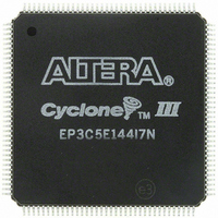
EP3C5E144I7N Altera, EP3C5E144I7N Datasheet - Page 150

EP3C5E144I7N
Manufacturer Part Number
EP3C5E144I7N
Description
IC CYCLONE III FPGA 5K 144 EQFP
Manufacturer
Altera
Series
Cyclone® IIIr
Datasheets
1.EP3C5F256C8N.pdf
(5 pages)
2.EP3C5F256C8N.pdf
(34 pages)
3.EP3C5F256C8N.pdf
(66 pages)
4.EP3C5F256C8N.pdf
(14 pages)
5.EP3C5F256C8N.pdf
(76 pages)
6.EP3C5E144I7N.pdf
(274 pages)
Specifications of EP3C5E144I7N
Number Of Logic Elements/cells
5136
Number Of Labs/clbs
321
Total Ram Bits
423936
Number Of I /o
94
Voltage - Supply
1.15 V ~ 1.25 V
Mounting Type
Surface Mount
Operating Temperature
-40°C ~ 100°C
Package / Case
144-EQFP
Family Name
Cyclone III
Number Of Logic Blocks/elements
5136
# I/os (max)
94
Frequency (max)
437.5MHz
Process Technology
65nm
Operating Supply Voltage (typ)
1.2V
Logic Cells
5136
Ram Bits
423936
Operating Supply Voltage (min)
1.15V
Operating Supply Voltage (max)
1.25V
Operating Temp Range
-40C to 100C
Operating Temperature Classification
Industrial
Mounting
Surface Mount
Pin Count
144
Package Type
EQFP
For Use With
544-2601 - KIT DEV CYCLONE III LS EP3CLS200544-2411 - KIT DEV NIOS II CYCLONE III ED.
Lead Free Status / RoHS Status
Lead free / RoHS Compliant
Number Of Gates
-
Lead Free Status / Rohs Status
Compliant
Other names
544-2557
Available stocks
Company
Part Number
Manufacturer
Quantity
Price
Company:
Part Number:
EP3C5E144I7N
Manufacturer:
Altera
Quantity:
135
Company:
Part Number:
EP3C5E144I7N
Manufacturer:
ALTERA32
Quantity:
345
Part Number:
EP3C5E144I7N
Manufacturer:
ALTERA/阿尔特拉
Quantity:
20 000
8–6
Table 8–1. Cyclone III Device DQS and DQ Bus Mode Support for Each Side of the Device (Part 4 of 4)
Table 8–2. Cyclone III LS Device DQS and DQ Bus Mode Support for Each Side of the Device
Cyclone III Device Handbook, Volume 1
EP3C120
Notes to
(1) This device package does not support ×32 or ×36 mode.
(2) For the top side of the device, RUP, RDN, PLLCLKOUT3n, and PLLCLKOUT3p pins are shared with the DQ or DM pins to gain ×8 DQ group. You
(3) There is no DM pin support for these groups.
(4) The RUP and RDN pins are shared with the DQ pins. You cannot use these groups if you are using the RUP and RDN pins for OCT calibration.
(5) The ×8 DQ group can be formed in Bank 2.
(6) The ×8 DQ group can be formed in Bank 5.
(7) There is no DM and BWS# pins support for these groups.
(8) The RUP pin is shared with the DQ pin to gain ×9 or ×18 DQ group. You cannot use these groups if you are using the RUP and RDN pins for
EP3CLS70
Device
Device
cannot use these groups if you are using the RUP and RDN pins for on-chip termination (OCT) calibration or if you are using PLLCLKOUT3n
and PLLCLKOUT3p.
OCT calibration.
Table
8–1:
484-pin FineLine BGA
780-pin FineLine BGA
484-pin FineLine
BGA/
484-pin Ultra FineLine
BGA
780-pin FineLine BGA
(2)
Table 8–2
Cyclone III LS device only.
Package
Package
lists the numbers of DQS or DQ groups supported on each side of the
Left
Right
Top
Bottom
Left
Right
Top
Bottom
Bottom
Bottom
Right
Right
Side
Side
Left
Left
Top
Top
Number
Number
Groups
Groups
of ×8
Chapter 8: External Memory Interfaces in the Cyclone III Device Family
×8
4
4
4
4
4
4
6
6
2
2
2
2
4
4
6
6
Number
Number
Groups
Groups
of ×9
×9
2
2
2
2
2
2
2
2
2
2
2
2
2
2
2
2
Cyclone III Device Family Memory Interfaces Pin Support
Number
Number
Groups
Groups
of ×16
×16
2
2
2
2
2
2
2
2
1
1
1
1
2
2
2
2
© January 2010 Altera Corporation
Number
Number
Groups
Groups
of ×18
×18
(Note 1)
2
2
2
2
2
2
2
2
1
1
1
1
2
2
2
2
Number
Number
Groups
Groups
of ×32
(Part 1 of 2)
×32
—
—
—
—
1
1
1
1
1
1
1
1
1
1
1
1
Number
Number
Groups
Groups
of ×36
×36
—
—
—
—
1
1
1
1
1
1
1
1
1
1
1
1


