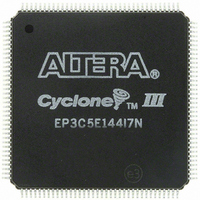
EP3C5E144I7N Altera, EP3C5E144I7N Datasheet - Page 214

EP3C5E144I7N
Manufacturer Part Number
EP3C5E144I7N
Description
IC CYCLONE III FPGA 5K 144 EQFP
Manufacturer
Altera
Series
Cyclone® IIIr
Datasheets
1.EP3C5F256C8N.pdf
(5 pages)
2.EP3C5F256C8N.pdf
(34 pages)
3.EP3C5F256C8N.pdf
(66 pages)
4.EP3C5F256C8N.pdf
(14 pages)
5.EP3C5F256C8N.pdf
(76 pages)
6.EP3C5E144I7N.pdf
(274 pages)
Specifications of EP3C5E144I7N
Number Of Logic Elements/cells
5136
Number Of Labs/clbs
321
Total Ram Bits
423936
Number Of I /o
94
Voltage - Supply
1.15 V ~ 1.25 V
Mounting Type
Surface Mount
Operating Temperature
-40°C ~ 100°C
Package / Case
144-EQFP
Family Name
Cyclone III
Number Of Logic Blocks/elements
5136
# I/os (max)
94
Frequency (max)
437.5MHz
Process Technology
65nm
Operating Supply Voltage (typ)
1.2V
Logic Cells
5136
Ram Bits
423936
Operating Supply Voltage (min)
1.15V
Operating Supply Voltage (max)
1.25V
Operating Temp Range
-40C to 100C
Operating Temperature Classification
Industrial
Mounting
Surface Mount
Pin Count
144
Package Type
EQFP
For Use With
544-2601 - KIT DEV CYCLONE III LS EP3CLS200544-2411 - KIT DEV NIOS II CYCLONE III ED.
Lead Free Status / RoHS Status
Lead free / RoHS Compliant
Number Of Gates
-
Lead Free Status / Rohs Status
Compliant
Other names
544-2557
Available stocks
Company
Part Number
Manufacturer
Quantity
Price
Company:
Part Number:
EP3C5E144I7N
Manufacturer:
Altera
Quantity:
135
Company:
Part Number:
EP3C5E144I7N
Manufacturer:
ALTERA32
Quantity:
345
Part Number:
EP3C5E144I7N
Manufacturer:
ALTERA/阿尔特拉
Quantity:
20 000
9–54
Figure 9–26. JTAG Configuration of Multiple Devices Using a Download Cable (2.5, 3.0, and 3.3-V V
Pins)
Notes to
(1) Connect these pull-up resistors to the V
(2) Connect the nCONFIG and MSEL[3..0] pins to support a non-JTAG configuration scheme. If you only use a JTAG configuration, connect the
(3) Pin 6 of the header is a V
(4) The nCE pin must be connected to ground or driven low for successful JTAG configuration.
(5) Power up the V
Cyclone III Device Handbook, Volume 1
Pin 1
10-Pin Male Header
Download Cable
nCONFIG pin to logic high and the MSEL[3..0] pins to ground. In addition, pull DCLK and DATA[0] either high or low, whichever is
convenient on your board.
MasterBlaster Serial/USB Communications Cable User
ByteBlaster II cables, this pin is connected to nCE when it is used for AS programming, otherwise it is a no connect.
to 2.5 V. Pin 4 of the header is a V
circuit boards, DC power supply, or 5.0 V from the USB cable. For this value, refer to the
Figure
V
CCA
(5)
10 kΩ
VIO
(3)
9–26:
1 kΩ
V
CC
CCA
of the ByteBlaster II, USB-Blaster, or ByteBlasterMV cable with a 2.5- V supply from V
V
CCA
10 kΩ
IO
(2)
(2)
(2)
(2)
(2)
reference voltage for the MasterBlaster output driver. V
V
CCIO
10
CC
(1)
DCLK
nST A TUS
DATA[0]
nCONFIG
MSEL[3..0]
nCEO
nCE
TDI
Chapter 9: Configuration, Design Security, and Remote System Upgrades in the Cyclone III Device Family
kΩ
power supply for the MasterBlaster cable. The MasterBlaster cable can receive power from either 5.0- or 3.3-V
TMS
(4)
Cyclone III Device
CCIO
Family
TCK
CONF_DONE
supply of the bank in which the pin resides.
TDO
V
Guide. In the ByteBlasterMV cable, this pin is a no connect. In the USB-Blaster and
CCIO
10
(1)
kΩ
(2)
(2)
(2)
(2)
(2)
V
CCIO
10
(1)
nST A TUS
DATA[0]
DCLK
nCONFIG
MSEL[3..0]
nCEO
nCE
TDI
kΩ
TMS
Cyclone III Device
(4)
IO
Family
must match the V
CONF_DONE
TCK
MasterBlaster Serial/USB Communications User
TDO
V
CCIO
10
CCA
CCA
(1)
kΩ
of the device. For this value, refer to the
. Third-party programmers must switch
© December 2009 Altera Corporation
(2)
(2)
(2)
(2)
(2)
V
CCIO
10
(1)
nST A TUS
DATA[0]
DCLK
nCONFIG
MSEL[3..0]
nCEO
nCE
TDI
CCIO
kΩ
TMS
(4)
Powering the JTAG
Cyclone III Device
Configuration Features
Family
TCK
CONF_DONE
TDO
V
CCIO
Guide.
10
(1)
kΩ


