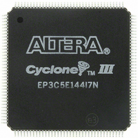
EP3C5E144I7N Altera, EP3C5E144I7N Datasheet - Page 220

EP3C5E144I7N
Manufacturer Part Number
EP3C5E144I7N
Description
IC CYCLONE III FPGA 5K 144 EQFP
Manufacturer
Altera
Series
Cyclone® IIIr
Datasheets
1.EP3C5F256C8N.pdf
(5 pages)
2.EP3C5F256C8N.pdf
(34 pages)
3.EP3C5F256C8N.pdf
(66 pages)
4.EP3C5F256C8N.pdf
(14 pages)
5.EP3C5F256C8N.pdf
(76 pages)
6.EP3C5E144I7N.pdf
(274 pages)
Specifications of EP3C5E144I7N
Number Of Logic Elements/cells
5136
Number Of Labs/clbs
321
Total Ram Bits
423936
Number Of I /o
94
Voltage - Supply
1.15 V ~ 1.25 V
Mounting Type
Surface Mount
Operating Temperature
-40°C ~ 100°C
Package / Case
144-EQFP
Family Name
Cyclone III
Number Of Logic Blocks/elements
5136
# I/os (max)
94
Frequency (max)
437.5MHz
Process Technology
65nm
Operating Supply Voltage (typ)
1.2V
Logic Cells
5136
Ram Bits
423936
Operating Supply Voltage (min)
1.15V
Operating Supply Voltage (max)
1.25V
Operating Temp Range
-40C to 100C
Operating Temperature Classification
Industrial
Mounting
Surface Mount
Pin Count
144
Package Type
EQFP
For Use With
544-2601 - KIT DEV CYCLONE III LS EP3CLS200544-2411 - KIT DEV NIOS II CYCLONE III ED.
Lead Free Status / RoHS Status
Lead free / RoHS Compliant
Number Of Gates
-
Lead Free Status / Rohs Status
Compliant
Other names
544-2557
Available stocks
Company
Part Number
Manufacturer
Quantity
Price
Company:
Part Number:
EP3C5E144I7N
Manufacturer:
Altera
Quantity:
135
Company:
Part Number:
EP3C5E144I7N
Manufacturer:
ALTERA32
Quantity:
345
Part Number:
EP3C5E144I7N
Manufacturer:
ALTERA/阿尔特拉
Quantity:
20 000
9–60
Cyclone III Device Handbook, Volume 1
Figure 9–30. Programming Serial Configuration Devices In-System Using the JTAG Interface
Notes to
(1) Connect the pull-up resistors to the V
(2) The MSEL pin settings vary for different configuration voltage standards and POR time. To connect MSEL[3..0]for
(3) Pin 6 of the header is a V
(4) The nCE pin must be connected to GND or driven low for successful JTAG configuration.
(5) The nCEO pin is left unconnected or used as a user I/O pin when it does not feed the nCE pin of another device.
(6) Power up the V
(7) Connect the series resistor at the near end of the serial configuration device.
(8) These are dual-purpose I/O pins. The nCSO pin functions as the FLASH_NCE pin in AP mode. The ASDO pin
ISP of the Configuration Device
In the second stage, the SFL design in the master device allows you to write the
configuration data for the device chain into the serial configuration device with the
Cyclone III device family JTAG interface. The JTAG interface sends the programming
data for the serial configuration device to the Cyclone III device family first. The
Cyclone III device family then uses the ASMI pins to send the data to the serial
configuration device.
AS configuration schemes, refer to
device. For this value, refer to the
this pin is a no connect. In USB-Blaster, ByteBlaster II, and Ethernet Blaster, this pin is connected to nCE when it is
used for AS programming, otherwise it is a no connect.
V
cable. The MasterBlaster cable can receive power from either 5.0- or 3.3-V circuit boards, DC power supply, or 5.0 V
from the USB cable. For this value, refer to the
functions as the DATA[1] pin in other AP and FPP modes.
CCA
Serial Configuration
. Third-party programmers must switch to 2.5 V. Pin 4 of the header is a V
Figure
Chapter 9: Configuration, Design Security, and Remote System Upgrades in the Cyclone III Device Family
Device
9–30:
CC
DCLK
DATA
ASDI
of the ByteBlaster II, USB-Blaster, ByteBlasterMV, or Ethernet Blaster cable with a 2.5-V supply from
nCS
V
CCIO
10
IO
(1)
V
25
kΩ
reference voltage for the MasterBlaster output driver. V
CCIO
Ω
10
(1)
(7)
V
kΩ
CCIO
MasterBlaster Serial/USB Communications Cable User
Table 9–7 on page
10
(1)
CCIO
GND
kΩ
(2)
N.C. (5)
supply of the bank in which the pin resides.
MasterBlaster Serial/USB Communications Cable User
Cyclone III Device Family
nCE
nCEO
nSTATUS
CONF_DONE
nCONFIG
MSEL[3..0]
DATA[0]
DCLK
nCSO (8)
ASDO (8)
(4)
9–11. Connect the MSEL pins directly to V
Loader
Serial
Flash
TDO
TMS
TCK
TDI
10
kΩ
V
CCA
© December 2009 Altera Corporation
CC
V
CCA
power supply for the MasterBlaster
10
1
IO
kΩ
kΩ
must match the V
GND
Guide. In ByteBlasterMV,
Download Cable 10-Pin Male
Pin 1
Configuration Features
Header (Top View)
CCA
GND
or GND.
V
Guide.
CCA
CCA
V
IO
(6)
of the
(3)
GND


