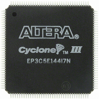
EP3C5E144I7N Altera, EP3C5E144I7N Datasheet - Page 141

EP3C5E144I7N
Manufacturer Part Number
EP3C5E144I7N
Description
IC CYCLONE III FPGA 5K 144 EQFP
Manufacturer
Altera
Series
Cyclone® IIIr
Datasheets
1.EP3C5F256C8N.pdf
(5 pages)
2.EP3C5F256C8N.pdf
(34 pages)
3.EP3C5F256C8N.pdf
(66 pages)
4.EP3C5F256C8N.pdf
(14 pages)
5.EP3C5F256C8N.pdf
(76 pages)
6.EP3C5E144I7N.pdf
(274 pages)
Specifications of EP3C5E144I7N
Number Of Logic Elements/cells
5136
Number Of Labs/clbs
321
Total Ram Bits
423936
Number Of I /o
94
Voltage - Supply
1.15 V ~ 1.25 V
Mounting Type
Surface Mount
Operating Temperature
-40°C ~ 100°C
Package / Case
144-EQFP
Family Name
Cyclone III
Number Of Logic Blocks/elements
5136
# I/os (max)
94
Frequency (max)
437.5MHz
Process Technology
65nm
Operating Supply Voltage (typ)
1.2V
Logic Cells
5136
Ram Bits
423936
Operating Supply Voltage (min)
1.15V
Operating Supply Voltage (max)
1.25V
Operating Temp Range
-40C to 100C
Operating Temperature Classification
Industrial
Mounting
Surface Mount
Pin Count
144
Package Type
EQFP
For Use With
544-2601 - KIT DEV CYCLONE III LS EP3CLS200544-2411 - KIT DEV NIOS II CYCLONE III ED.
Lead Free Status / RoHS Status
Lead free / RoHS Compliant
Number Of Gates
-
Lead Free Status / Rohs Status
Compliant
Other names
544-2557
Available stocks
Company
Part Number
Manufacturer
Quantity
Price
Company:
Part Number:
EP3C5E144I7N
Manufacturer:
Altera
Quantity:
135
Company:
Part Number:
EP3C5E144I7N
Manufacturer:
ALTERA32
Quantity:
345
Part Number:
EP3C5E144I7N
Manufacturer:
ALTERA/阿尔特拉
Quantity:
20 000
Chapter 7: High-Speed Differential Interfaces in the Cyclone III Device Family
Design Guidelines
Figure 7–16. Cyclone III Device Family High-Speed I/O Timing Budget
Note to
(1) The equation for the high-speed I/O timing budget is:
Design Guidelines
Differential Pad Placement Guidelines
Board Design Considerations
© December 2009
Period
Figure
=
7–16:
0.5
f
f
Internal Clock Period
Altera Corporation
×
TCCS
Figure 7–16
For more information, refer to the
Device Data Sheet
This section provides guidelines for designing with the Cyclone III device family.
To maintain an acceptable noise level on the V
restrictions on the placement of single-ended I/O pins in relation to differential pads.
For more information about the guidelines on placing single-ended pads with respect
to differential pads in the Cyclone III device family, refer to the
Features
This section explains how to achieve the optimal performance from the Cyclone III
device family I/O interface and ensure first-time success in implementing a
functional design with optimal signal quality. You must consider the critical issues of
controlled impedance of traces and connectors, differential routing, and termination
techniques to get the best performance from the Cyclone III device family.
Use the following general guidelines for improved signal quality:
■
■
■
■
+
RSKM
Base board designs on controlled differential impedance. Calculate and compare
all parameters, such as trace width, trace thickness, and the distance between two
differential traces.
Maintain equal distance between traces in differential I/O standard pairs as much
as possible. Routing the pair of traces close to each other maximizes the
common-mode rejection ratio (CMRR).
Longer traces have more inductance and capacitance. These traces must be as
short as possible to limit signal integrity issues.
Place termination resistors as close to receiver input pins as possible.
chapter.
+
SW
shows the Cyclone III device family high-speed I/O timing budget.
0.5 × TCCS
+
RSKM
chapters in volume 2 of the Cyclone III Device Handbook.
RSKM
+
0.5
×
TCCS.
Cyclone III Device Data Sheet
SW
(Note 1)
CCIO
supply, you must observe some
RSKM
Cyclone III Device Handbook, Volume 1
0.5 × TCCS
and
Cyclone III Device I/O
Cyclone III LS
7–17


