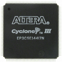
EP3C5E144I7N Altera, EP3C5E144I7N Datasheet - Page 146

EP3C5E144I7N
Manufacturer Part Number
EP3C5E144I7N
Description
IC CYCLONE III FPGA 5K 144 EQFP
Manufacturer
Altera
Series
Cyclone® IIIr
Datasheets
1.EP3C5F256C8N.pdf
(5 pages)
2.EP3C5F256C8N.pdf
(34 pages)
3.EP3C5F256C8N.pdf
(66 pages)
4.EP3C5F256C8N.pdf
(14 pages)
5.EP3C5F256C8N.pdf
(76 pages)
6.EP3C5E144I7N.pdf
(274 pages)
Specifications of EP3C5E144I7N
Number Of Logic Elements/cells
5136
Number Of Labs/clbs
321
Total Ram Bits
423936
Number Of I /o
94
Voltage - Supply
1.15 V ~ 1.25 V
Mounting Type
Surface Mount
Operating Temperature
-40°C ~ 100°C
Package / Case
144-EQFP
Family Name
Cyclone III
Number Of Logic Blocks/elements
5136
# I/os (max)
94
Frequency (max)
437.5MHz
Process Technology
65nm
Operating Supply Voltage (typ)
1.2V
Logic Cells
5136
Ram Bits
423936
Operating Supply Voltage (min)
1.15V
Operating Supply Voltage (max)
1.25V
Operating Temp Range
-40C to 100C
Operating Temperature Classification
Industrial
Mounting
Surface Mount
Pin Count
144
Package Type
EQFP
For Use With
544-2601 - KIT DEV CYCLONE III LS EP3CLS200544-2411 - KIT DEV NIOS II CYCLONE III ED.
Lead Free Status / RoHS Status
Lead free / RoHS Compliant
Number Of Gates
-
Lead Free Status / Rohs Status
Compliant
Other names
544-2557
Available stocks
Company
Part Number
Manufacturer
Quantity
Price
Company:
Part Number:
EP3C5E144I7N
Manufacturer:
Altera
Quantity:
135
Company:
Part Number:
EP3C5E144I7N
Manufacturer:
ALTERA32
Quantity:
345
Part Number:
EP3C5E144I7N
Manufacturer:
ALTERA/阿尔特拉
Quantity:
20 000
8–2
Cyclone III Device Family Memory Interfaces Pin Support
Data and Data Clock/Strobe Pins
Cyclone III Device Handbook, Volume 1
f
1
1
1
Cyclone III device family uses data (DQ), data strobe (DQS), clock, command, and
address pins to interface with external memory. Some memory interfaces use the data
mask (DM) or byte write select (BWS#) pins to enable data masking. This section
describes how Cyclone III device family supports all these different pins.
Cyclone III device family data pins for external memory interfaces are called D for
write data, Q for read data, or DQ for shared read and write data pins. The read-data
strobes or read clocks are called DQS pins. Cyclone III device family supports both
bidirectional data strobes and unidirectional read clocks. Depending on the external
memory standard, the DQ and DQS are bidirectional signals (in DDR2 and
DDR SDRAM) or unidirectional signals (in QDR II SRAM). Connect the bidirectional
DQ data signals to the same Cyclone III device family DQ pins. For unidirectional D or
Q signals, connect the read-data signals to a group of DQ pins and the write-data
signals to a different group of DQ pins.
In QDR II SRAM, the Q read-data group must be placed at a different V
location from the D write-data group, command, or address pins.
In Cyclone III device family, DQS is used only during write mode in DDR2 and
DDR SDRAM interfaces. Cyclone III device family ignores DQS as the read-data
strobe because the PHY internally generates the read capture clock for read mode.
However, you must connect the DQS pin to the DQS signal in DDR2 and
DDR SDRAM interfaces, or to the CQ signal in QDR II SRAM interfaces.
Cyclone III device family does not support differential strobe pins, which is an
optional feature in the DDR2 SDRAM device.
When you use the Altera Memory Controller MegaCore
you. For more information about the memory interface data path, refer to
External Memory
ALTMEMPHY is a self-calibrating megafunction, enhanced to simplify the
implementation of the read-data path in different memory interfaces. The
auto-calibration feature of ALTMEMPHY provides ease-of-use by optimizing clock
phases and frequencies across process, voltage, and temperature (PVT) variations.
You can save on the global clock resources in Cyclone III device family through the
ALTMEMPHY megafunction because you are not required to route the DQS signals
on the global clock buses (because DQS is ignored for read capture).
Resynchronization issues do not arise because no transfer occurs from the memory
domain clock (DQS) to the system domain for capturing data DQ.
All I/O banks in Cyclone III device family can support DQ and DQS signals with DQ-
bus modes of ×8, ×9, ×16, ×18, ×32, and ×36. DDR2 and DDR SDRAM interfaces use
×8 mode DQS group regardless of the interface width. For wider interface, you can
use multiple ×8 DQ groups to achieve the desired width requirement.
Interfaces.
Chapter 8: External Memory Interfaces in the Cyclone III Device Family
Cyclone III Device Family Memory Interfaces Pin Support
®
, the PHY is instantiated for
© January 2010 Altera Corporation
REF
Literature:
bank


