EP3C5E144I7N Altera, EP3C5E144I7N Datasheet - Page 158
EP3C5E144I7N
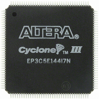
Manufacturer Part Number
EP3C5E144I7N
Description
IC CYCLONE III FPGA 5K 144 EQFP
Manufacturer
Altera
Series
Cyclone® IIIr
Datasheets
1.EP3C5F256C8N.pdf
(5 pages)
2.EP3C5F256C8N.pdf
(34 pages)
3.EP3C5F256C8N.pdf
(66 pages)
4.EP3C5F256C8N.pdf
(14 pages)
5.EP3C5F256C8N.pdf
(76 pages)
6.EP3C5E144I7N.pdf
(274 pages)
Specifications of EP3C5E144I7N
Number Of Logic Elements/cells
5136
Number Of Labs/clbs
321
Total Ram Bits
423936
Number Of I /o
94
Voltage - Supply
1.15 V ~ 1.25 V
Mounting Type
Surface Mount
Operating Temperature
-40°C ~ 100°C
Package / Case
144-EQFP
Family Name
Cyclone III
Number Of Logic Blocks/elements
5136
# I/os (max)
94
Frequency (max)
437.5MHz
Process Technology
65nm
Operating Supply Voltage (typ)
1.2V
Logic Cells
5136
Ram Bits
423936
Operating Supply Voltage (min)
1.15V
Operating Supply Voltage (max)
1.25V
Operating Temp Range
-40C to 100C
Operating Temperature Classification
Industrial
Mounting
Surface Mount
Pin Count
144
Package Type
EQFP
For Use With
544-2601 - KIT DEV CYCLONE III LS EP3CLS200544-2411 - KIT DEV NIOS II CYCLONE III ED.
Lead Free Status / RoHS Status
Lead free / RoHS Compliant
Number Of Gates
-
Lead Free Status / Rohs Status
Compliant
Other names
544-2557
Available stocks
Company
Part Number
Manufacturer
Quantity
Price
Company:

Part Number:
EP3C5E144I7N
Manufacturer:
Altera
Quantity:
135
Company:
Part Number:
EP3C5E144I7N
Manufacturer:
ALTERA32
Quantity:
345
Part Number:
EP3C5E144I7N
Manufacturer:
ALTERA/阿尔特拉
Quantity:
20 000


8–14
Chapter Revision History
Table 8–3. Chapter Revision History
Cyclone III Device Handbook, Volume 1
January 2010
December 2009
July 2009
June 2009
October 2008
May 2008
July 2007
March 2007
Date
f
For more information about Cyclone III device family PLL, refer to the
and PLLs in Cyclone III Devices
Table 8–3
Version
2.3
2.2
2.1
2.0
1.3
1.2
1.1
1.0
lists the revision history for this chapter.
■
■
Minor changes to the text.
Made minor correction to the part number.
■
■
■
■
■
■
■
■
■
■
■
■
■
■
Initial release.
Removed Tables 8-1, 8-2, 8-3, and 8-4.
Changed links to reference
Updated chapter part number.
Updated “Introduction” on page 8–1.
Updated Table 8–1 on page 8–1, Table 8–2 on page 8–2, Table 8–3 on
page 8–3, Table 8–4 on page 8–4, and Table 8–5 on page 8–7. Updated notes
to Table 8–6 on page 8–10. Updated “Data and Data Clock/Strobe Pins” on
page 8–5.
Updated note to Figure 8–2 on page 8–12.
Updated “Optional Parity, DM, and Error Correction Coding Pins” on
page 8–13.
Updated “Address and Control/Command Pins” on page 8–14.
Updated “Introduction”, “DDR Input Registers” and “Conclusion” sections.
Updated chapter to new template.
Added (Note 4) to Figure 8–3.
Updated Table 8–3 and Table 8-5. Added new Table 8–4.
Updated (Note 1) to Figure 8-4. Updated Figure 8–5 and 8–14.
Updated “Data and Data Clock/Strobe Pins” section.
Updated Table 8–5.
Added chapter TOC and “Referenced Documents” section.
chapter.
Chapter 8: External Memory Interfaces in the Cyclone III Device Family
Literature: External Memory Interfaces
Changes Made
© January 2010 Altera Corporation
Chapter Revision History
Clock Networks
.
Related parts for EP3C5E144I7N
Image
Part Number
Description
Manufacturer
Datasheet
Request
R

Part Number:
Description:
Cyclone III Device Data Sheet
Manufacturer:
ALTERA [Altera Corporation]
Datasheet:

Part Number:
Description:
CYCLONE II STARTER KIT EP2C20N
Manufacturer:
Altera
Datasheet:


Part Number:
Description:
CPLD, EP610 Family, ECMOS Process, 300 Gates, 16 Macro Cells, 16 Reg., 16 User I/Os, 5V Supply, 35 Speed Grade, 24DIP
Manufacturer:
Altera Corporation
Datasheet:
Part Number:
Description:
CPLD, EP610 Family, ECMOS Process, 300 Gates, 16 Macro Cells, 16 Reg., 16 User I/Os, 5V Supply, 15 Speed Grade, 24DIP
Manufacturer:
Altera Corporation
Datasheet:
Part Number:
Description:
Manufacturer:
Altera Corporation
Datasheet:
Part Number:
Description:
CPLD, EP610 Family, ECMOS Process, 300 Gates, 16 Macro Cells, 16 Reg., 16 User I/Os, 5V Supply, 30 Speed Grade, 24DIP
Manufacturer:
Altera Corporation
Datasheet:
Part Number:
Description:
High-performance, low-power erasable programmable logic devices with 8 macrocells, 10ns
Manufacturer:
Altera Corporation
Datasheet:
Part Number:
Description:
High-performance, low-power erasable programmable logic devices with 8 macrocells, 7ns
Manufacturer:
Altera Corporation
Datasheet:
Part Number:
Description:
Classic EPLD
Manufacturer:
Altera Corporation
Datasheet:
Part Number:
Description:
High-performance, low-power erasable programmable logic devices with 8 macrocells, 10ns
Manufacturer:
Altera Corporation
Datasheet:
Part Number:
Description:
Manufacturer:
Altera Corporation
Datasheet:
Part Number:
Description:
Manufacturer:
Altera Corporation
Datasheet:
Part Number:
Description:
Manufacturer:
Altera Corporation
Datasheet: